

Full Name: High Numerical Aperture Extreme Ultraviolet Lithography
Abbreviation: High-NA EUV
Technology Type: Advanced semiconductor photolithography
Developed By: ASML, Zeiss, in collaboration with Intel, TSMC, imec, and others
First Deployment Target: Intel (expected ~2025–2026)
Main Use: Sub-2nm logic node patterning
Predecessor: EUV (0.33 NA systems – ASML NXE series)
Tool Platform: ASML EXE series (e.g., EXE:5000, EXE:5200)
Key Collaborators: ASML, Zeiss, Intel, imec, TSMC, Samsung
Overview
High-NA EUV is the next major advancement in photolithography technology designed to extend the scalability of extreme ultraviolet (EUV) lithography into the sub-2nm process node era. “NA” stands for numerical aperture, a measure of the lens system’s resolution power.
While today’s production EUV systems use a 0.33 NA lens, High-NA EUV will increase that to 0.55 NA, dramatically improving the resolution and enabling single-exposure patterning at tighter pitches. It is considered a key enabler for advanced semiconductor nodes like Intel 14A, TSMC A14, and beyond.
What is Numerical Aperture (NA)?
Numerical Aperture (NA) in lithography is a measure of a system’s ability to focus light into fine patterns. Higher NA means:
-
Better resolution
-
Ability to print smaller features
-
Tighter pitches and higher density patterns
The Rayleigh resolution formula helps express this:
Minimum Feature Size=k1⋅λNA\text{Minimum Feature Size} = k_1 \cdot \frac{\lambda}{\text{NA}}
Where:
-
λ\lambda is the wavelength (13.5 nm for EUV)
-
NA is numerical aperture
-
k1k_1 is a process constant
By increasing NA from 0.33 to 0.55, High-NA EUV can pattern features ~70% smaller with the same process complexity.
Technical Features
1. Lens System
-
Developed by Carl Zeiss SMT, the High-NA EUV lens features a larger mirror angle and numerical aperture of 0.55.
-
Uses Schwarzschild optics (multi-mirror reflective system) adapted to handle higher magnification and tighter tolerances.
2. Higher Resolution
-
Targeted for 20nm pitch single-pattern capability (vs. ~30nm for 0.33 NA).
-
Reduces the need for multi-patterning, improving throughput and design rule simplification.
3. EUV Source and Power
-
Based on the same 13.5 nm wavelength from tin-based plasma sources (LPP).
-
Requires higher EUV power and improved optics to compensate for smaller field size.
4. Field Size Reduction
-
High-NA systems have a smaller slit and field size, necessitating changes in chip layout strategy.
-
Die stitching techniques may be used to create large dies from smaller fields.
5. Metrology and Mask Challenges
-
Masks need higher precision and defect control.
-
Pellicles (protective membranes) must be thinner and more transparent to EUV.
-
New resist materials and line-edge roughness (LER) controls are required.
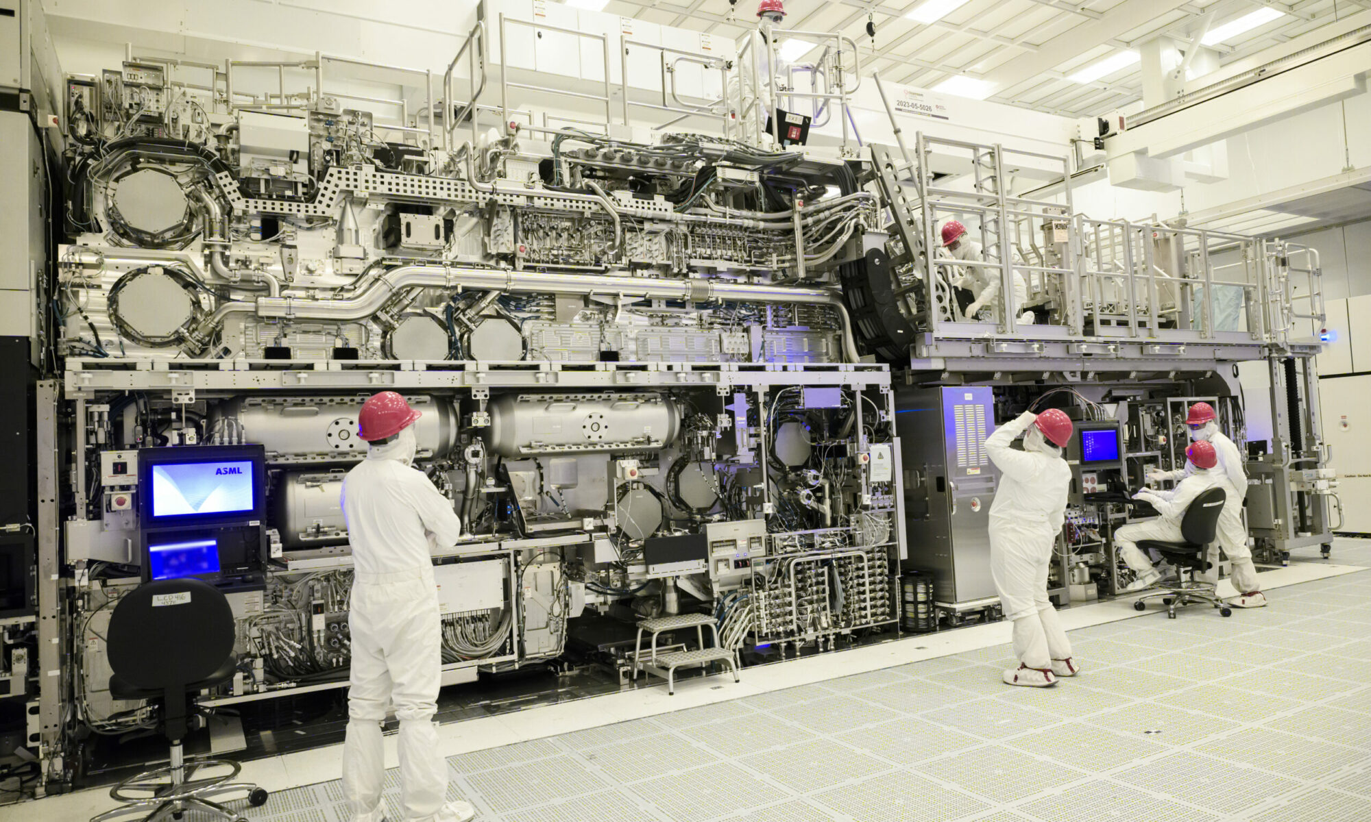
Tool Platform: ASML EXE Series
| Tool | NA | First Shipments | Customers |
|---|---|---|---|
| NXE series | 0.33 | 2016–ongoing | All leading fabs |
| EXE:5000 | 0.55 | 2023 (Intel) | Intel, imec |
| EXE:5200 | 0.55 | 2025+ (HVM) | Intel, TSMC, Samsung (planned) |
-
The ASML EXE:5000 is a development tool delivered to Intel for early R&D.
-
The EXE:5200 is the production model, capable of high-volume manufacturing (HVM) by 2025–2026.
Use Cases and Node Targets
High-NA EUV is expected to be deployed for the following nodes and beyond:
| Company | Node | High-NA Use Target |
|---|---|---|
| Intel | 14A | First adopter (2025–2026) |
| TSMC | A14 or N1 | Research underway (2026+) |
| Samsung | SF2 / SF1.4 | Expected in roadmap (TBD) |
| imec | Various R&D nodes | Process pathfinding |
Initial use cases:
-
Logic transistor scaling (GAA, CFET)
-
Interconnect scaling with tighter metal pitches
-
Chiplet I/O optimization (via UCIe + denser bonding)
Benefits
| Benefit | Description |
|---|---|
| Higher Resolution | Enables smaller features and denser designs |
| Fewer Multi-Patterning Steps | Simplifies manufacturing complexity |
| Better Edge Placement Accuracy | Crucial for yield and scaling |
| Enabler for 1.5nm and Beyond | Extends Moore’s Law scalability |
| Improved Performance & Power | Enables transistor and interconnect optimizations |
Challenges
| Challenge | Explanation |
|---|---|
| Tool Cost | Over $300 million per tool, high capital expenditure |
| Field Size Reduction | Smaller exposure areas complicate layout planning |
| New Resists Needed | High-NA requires stiffer and more precise photoresists |
| Mask and Pellicle Engineering | Demands ultra-clean and precise optics |
| Throughput Concerns | Higher resolution = more exposure time, affects wafer-per-hour (WPH) |
Intel’s Leadership in High-NA EUV
-
Intel is the lead customer for High-NA EUV.
-
First EXE:5000 tool delivered to Oregon R&D fab in 2023.
-
Planning to use High-NA for Intel 14A and future process nodes.
-
Intel collaborates closely with ASML and imec to optimize High-NA patterning, resist materials, and tool operation.
Future Outlook
-
High-NA EUV is a critical enabler for sustaining Moore’s Law into the angstrom era.
-
Could be combined with other techniques like CFET, advanced packaging, and hybrid bonding to enable future logic scaling.
-
Research into even higher NA, EUV double patterning, and patterned mask techniques continues at imec and national labs.
Conclusion
High-NA EUV represents the most advanced lithography platform ever developed, pushing optical resolution beyond previous limits. While it brings engineering, cost, and integration challenges, its potential to enable sub-2nm logic nodes with better PPA (Performance, Power, Area) scaling is unmatched.
As fabs like Intel and TSMC race toward the angstrom era, High-NA EUV will play a foundational role in next-generation chip manufacturing and semiconductor innovation.


Things From Intel 10K That Make You Go …. Hmmmm