

Full Name: Gate-All-Around Field-Effect Transistor
Also Known As: Gate-All-Around FET, Nanosheet FET, Nanowire FET
Category: Advanced 3D CMOS Transistor
Predecessor: FinFET (Tri-Gate Transistor)
Successors/Subtypes: Nanosheet FET, MBCFET (Samsung), RibbonFET (Intel), Forksheet FET
First Commercial Use: Samsung 3nm (2022)
Primary Application: Sub-5nm logic transistor scaling for SoCs, CPUs, GPUs, AI accelerators
Overview
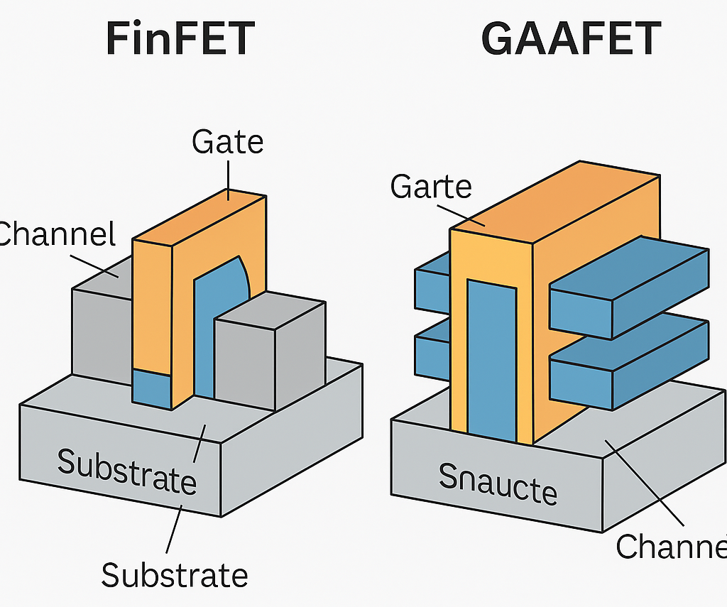
A GAAFET is a transistor architecture in which the gate completely surrounds the channel on all four sides, offering superior electrostatic control, reduced leakage, and enhanced scalability compared to FinFETs. It is widely regarded as the natural successor to FinFETs for technology nodes below 5nm, where traditional FinFETs begin to encounter physical and performance limitations.
The GAAFET architecture allows for wider performance tuning, better short-channel control, and more compact scaling, making it ideal for high-performance and low-power semiconductor designs in the AI, mobile, automotive, and HPC markets.
Architecture
-
GAAFETs use stacked horizontal nanosheets or nanowires as the transistor’s channel.
-
The gate material wraps around each channel on all sides (top, bottom, and sides), ensuring maximum gate control.
-
Unlike FinFETs (which use vertical fins), nanosheet GAAFETs use horizontally stacked sheets that resemble ribbons or plates.
Key Elements:
-
Channel: Nanosheet or nanowire silicon layer
-
Gate: Fully wraps around the channel
-
Source/Drain: Contacted on either side of the nanosheet stack
-
Spacer: Controls parasitic capacitance
-
Epitaxy: Enables selective growth of nanosheets
Advantages over FinFET
| Feature | FinFET | GAAFET |
|---|---|---|
| Gate control | 3-sided (tri-gate) | 4-sided (gate-all-around) |
| Channel geometry | Vertical fin | Horizontal nanosheet |
| Short-channel suppression | Good | Excellent |
| Leakage current | Low | Lower |
| Performance tuning | Quantized (fin count) | Continuous (sheet width) |
| Area scaling | Limited | Improved |
| Design flexibility | Moderate | High |
GAAFET Variants and Terminology
| Name | Description | Developer |
|---|---|---|
| Nanosheet FET | Horizontal wide sheets for tunable performance | TSMC, IBM, Intel |
| Nanowire FET | Cylindrical thin wires (early research form) | Academia, IBM |
| MBCFET | Multi-Bridge Channel FET (sheet-based) | Samsung |
| RibbonFET | Intel’s proprietary GAAFET with stacked ribbons | Intel (20A/18A) |
| Forksheet FET | Gate-first variation for tighter layouts | Imec (future node) |
Technology Roadmap and Adoption Timeline
| Year | Event |
|---|---|
| 2019 | Samsung announces MBCFET as FinFET successor |
| 2020 | IBM demonstrates stacked nanosheet GAAFET at 5nm |
| 2022 | Samsung begins mass production of 3nm MBCFET |
| 2023–24 | Intel preps RibbonFET for Intel 20A / 18A |
| 2025+ | TSMC expected to launch N2 node with nanosheet GAAFET |
| Late 2020s | Forksheet and CFET (Complementary FET) in R&D roadmap |
Design Considerations
-
Sheet width can be adjusted for performance tuning (wider for high drive current, narrower for low power)
-
Can accommodate multiple sheets per transistor, stacked vertically
-
Better Vt tuning and threshold voltage control than FinFET
-
Higher process complexity, especially in nanosheet release and uniformity
-
Requires advanced EUV lithography, selective epitaxy, and dielectric engineering
Challenges
| Area | Challenge |
|---|---|
| Manufacturing | Complex sheet release, spacing, and alignment |
| Parasitics | Capacitance and resistance at high aspect ratios |
| Yield | Increased risk of defect density and variability |
| Tooling | Requires advanced process control and EUV layers |
| Design Flow | Needs new standard cells, PDKs, and SPICE models |
Applications
GAAFETs are targeted for:
-
Flagship mobile SoCs (e.g., smartphones, tablets)
-
High-performance CPUs and GPUs
-
AI/ML accelerators
-
Automotive-grade SoCs
-
Advanced chiplets and 3D ICs
GAAFET vs. Other Transistor Types
| Feature | Planar CMOS | FinFET | GAAFET | Forksheet | CFET (future) |
|---|---|---|---|---|---|
| Gate control | 1-sided | 3-sided | 4-sided | 4-sided (tight pitch) | 4-sided (P+N stacked) |
| Introduced (mass) | 1990s | 2011 | 2022 | ~2027 | ~2030 |
| Scalability limit | ~28nm | ~3nm | ~1.5nm | ~1.0nm | Sub-1nm |
| 3D Integration | ❌ | ⚠️ | ✅ | ✅ | ✅ |
Outlook and Future
GAAFET is currently the most promising mainstream transistor architecture beyond 5nm, with strong momentum across all major foundries. In the coming years:
-
GAAFET will dominate at 3nm and 2nm nodes
-
May eventually be replaced or complemented by Forksheet FET and CFETs (Complementary FETs) for tighter vertical scaling
-
Will be central to chiplet designs, 3D stacking, and advanced packaging
Conclusion
GAAFET represents the next evolution of CMOS transistors, offering superior control, power efficiency, and design flexibility compared to FinFET. As the semiconductor industry continues to push physical and economic limits, GAAFETs are expected to enable Moore’s Law into the sub-3nm and possibly sub-1nm era.
🕒 GAAFET Technology Timeline
| Year | Milestone |
|---|---|
| 1998–2002 | Academic foundation: Nanowire and gate-all-around FET concepts are published in research from institutions like UC Berkeley and IMEC. |
| 2010–2015 | Early nanosheet and nanowire prototypes demonstrated by IBM, IMEC, and academic labs. Industry begins planning for FinFET successors. |
| 2017 | Samsung announces MBCFET (Multi-Bridge Channel FET), a GAAFET-based technology using nanosheets instead of nanowires for better performance and manufacturability. |
| 2019 | IBM and Samsung demonstrate stacked nanosheet GAAFETs at 5nm, showing improved electrostatic control vs. FinFET. |
| 2020 | Samsung completes test chip tapeouts at 3nm using MBCFET. |
| 2022 | Samsung begins volume production of 3nm chips using MBCFET (first commercial GAAFET deployment in the world). |
| 2023 | Samsung ramps up 3nm Gen 2 (SF3) with improved yields; Intel introduces RibbonFET in technical disclosures for Intel 20A / 18A. |
| 2024 | TSMC finalizes development for N2 node (2nm), its first node using nanosheet GAAFET, targeting 2025–2026 production. |
| 2025 | Intel expected to begin production of RibbonFET at Intel 18A, using horizontal nanosheet GAAFETs with PowerVia (backside power). |
| 2026+ | TSMC ramps N2 GAAFET production; GAAFET becomes mainstream for advanced logic below 3nm across foundries. |
| 2027–2030 | Research into Forksheet FET and CFET (Complementary FET) begins maturing as potential GAAFET successors. |
📌 Summary Highlights:
-
🧪 Invented in academia: ~2000
-
🏭 First commercial use: Samsung 3nm MBCFET (2022)
-
🔄 Industry transition: 2022–2025, as FinFET tapers off at 5nm
-
🔮 Future evolution: Forksheet FETs (~2027), CFETs (~2030)


Captain America: Can Elon Musk Save America’s Chip Manufacturing Industry?