

Full Name: Fin Field-Effect Transistor
Also Known As: 3D Tri-Gate Transistor, Multi-Gate FET
Category: Advanced CMOS Transistor Technology
Introduced by Industry: ~2011 (Intel 22nm)
Invented by: Chenming Hu and colleagues at UC Berkeley (1999)
Replaced: Planar CMOS Transistors
Successor Technology: Gate-All-Around FETs (GAAFET), Nanosheet FETs, MBCFET, RibbonFET
Overview
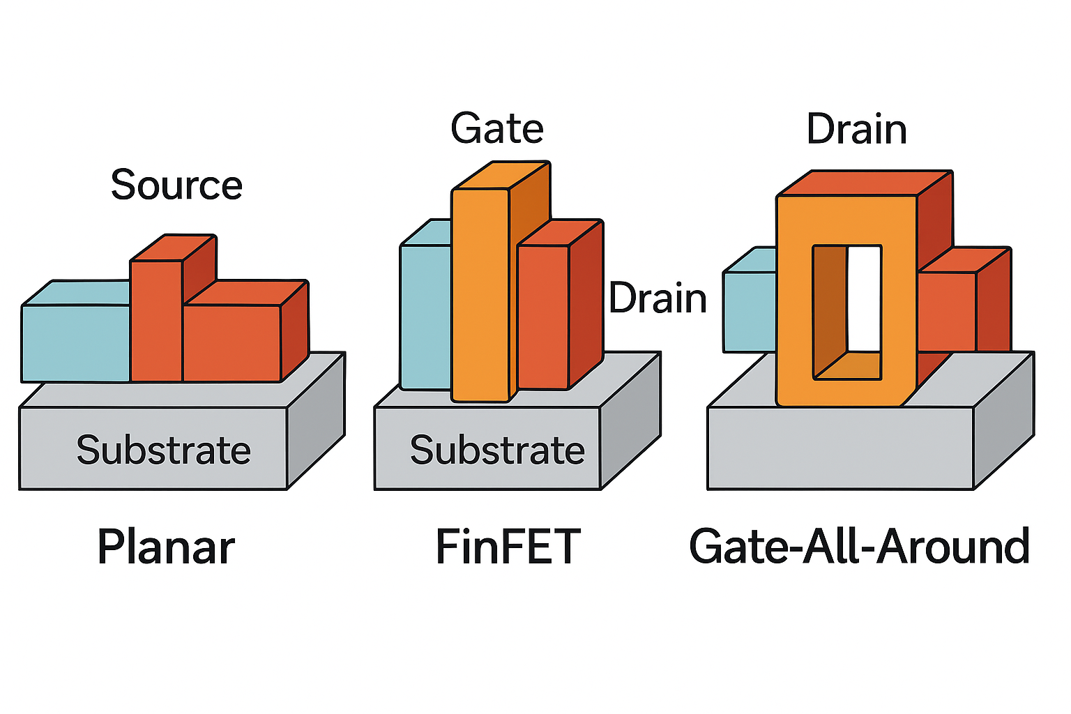
FinFET is a type of non-planar, 3D transistor used in advanced semiconductor manufacturing nodes starting from 22nm and below. Unlike traditional planar CMOS transistors, which are flat and lie on the substrate, FinFETs feature a fin-shaped 3D channel that rises above the substrate and is surrounded on multiple sides by the gate.
This architecture offers better electrostatic control, lower leakage current, and enhanced drive strength, allowing chipmakers to continue transistor scaling beyond the limits of planar technologies.
Structure and Operation
In a FinFET:
-
The channel is a thin silicon fin standing vertically above the substrate.
-
The gate wraps around the fin on three sides (top and both sidewalls).
-
The source and drain are formed at either end of the fin.
-
Multiple fins can be connected in parallel to enhance current drive.
This results in a tri-gate effect—with more surface area for the gate to control the channel—leading to improved:
-
Subthreshold slope
-
Drain-induced barrier lowering (DIBL)
-
Short channel effects suppression
Key Benefits over Planar Transistors
| Feature | Planar CMOS | FinFET |
|---|---|---|
| Gate control | Single-side (top) | Three-sided wrap |
| Leakage current | Higher | Much lower |
| Drive current | Moderate | Higher per fin |
| Scalability (beyond 20nm) | Difficult | Excellent |
| Channel length control | Limited | Improved |
| Subthreshold slope | ~90 mV/dec | ~70 mV/dec |
History and Development Timeline
| Year | Milestone |
|---|---|
| 1999 | FinFET proposed by Chenming Hu at UC Berkeley |
| 2002 | First academic demonstration of functional FinFETs |
| 2011 | Intel introduces 22nm FinFET (“Tri-Gate”) in production |
| 2014–2016 | FinFET adopted by TSMC (16nm), Samsung (14nm) |
| 2018+ | FinFET becomes dominant for 16nm, 10nm, 7nm, 5nm nodes |
| 2020s | FinFET gradually replaced by GAA for 3nm and below |
Foundry Adoption
| Company | First FinFET Node | Notable Products |
|---|---|---|
| Intel | 22nm (2011) | Ivy Bridge, Haswell CPUs |
| TSMC | 16nm (2015) | A9, Snapdragon 820 |
| Samsung | 14nm (2015) | Exynos 7420 |
| GlobalFoundries | 14nm (2016, licensed) | AMD Ryzen, IBM chips |
Today, FinFETs are widely used at 16nm, 12nm, 10nm, 7nm, and 5nm across all major foundries.
Design and Scaling Challenges
Despite their advantages, FinFETs face several issues as scaling continues:
-
Fin height vs. pitch trade-off limits further performance scaling
-
Increased parasitic capacitance due to taller fin structures
-
Complex lithography and patterning (multiple patterning required)
-
Harder SRAM scaling
-
Difficult to tune threshold voltage with narrow fin width
These challenges have led to the development of Gate-All-Around FETs (GAAFETs), which provide even better electrostatic control by fully surrounding the channel.
FinFET vs. GAAFET
| Feature | FinFET | GAAFET (e.g., nanosheet, MBCFET) |
|---|---|---|
| Gate control | 3-sided | 4-sided (fully surrounding) |
| Channel shape | Vertical fin | Stacked horizontal nanosheets |
| Performance tunability | Discrete via # of fins | Continuous via sheet width |
| Scalability | Limited beyond 5nm | Better for sub-3nm |
| Leakage | Low | Even lower |
Applications and Use Cases
FinFETs have powered billions of consumer and enterprise devices, including:
-
Smartphones and mobile SoCs
-
High-performance CPUs and GPUs
-
AI accelerators (NVIDIA, Google TPU)
-
Automotive SoCs and microcontrollers
-
5G baseband and RFICs
-
Data center processors and accelerators
Manufacturing Considerations
-
Fabricated using Fin patterning, gate-last process, and HKMG (high-k metal gate) stacks
-
Typically use double/triple/quad patterning at advanced nodes
-
Design techniques include multi-fin cells, fin depopulation, and fin pitch modulation
Future Outlook
While FinFET has been the workhorse of the industry for over a decade, it is reaching its physical and economic limits below 5nm. As of 2024–2025:
-
TSMC and Samsung are transitioning to nanosheet GAAFETs at 3nm and 2nm
-
Intel is moving to RibbonFET (a type of GAAFET) for its Intel 20A and 18A nodes
-
Some foundries will continue offering FinFET at mature nodes for cost-sensitive products
FinFET will remain relevant in low-cost, embedded, and trailing-edge applications for years to come.
Conclusion
FinFETs represent a revolutionary shift in transistor design, enabling continued CMOS scaling into the sub-20nm era. By moving to a 3D structure with multi-gate control, FinFETs allowed the semiconductor industry to push Moore’s Law well beyond its expected limits. While they are now being succeeded by GAAFETs in bleeding-edge nodes, FinFETs will remain an integral part of modern silicon for a wide range of applications.
🕒 FinFET Technology Timeline
| Year | Milestone |
|---|---|
| 1999 | FinFET invention: Proposed by Chenming Hu and team at UC Berkeley to overcome short-channel effects in scaled CMOS |
| 2002 | First working FinFET prototypes demonstrated in academic labs, showing better subthreshold control |
| 2005–2010 | Academic and foundry R&D intensifies; Intel, IBM, TSMC begin prototyping for future nodes |
| 2011 | Intel introduces 22nm Tri-Gate FinFET (Ivy Bridge CPUs), marking first commercial FinFET deployment |
| 2014 | TSMC 16nm FinFET hits production (Apple A9, various mobile SoCs) |
| 2015 | Samsung launches 14nm FinFET in Exynos and Snapdragon processors |
| 2016–2018 | FinFET dominates at 16nm, 14nm, 10nm, and 7nm nodes (TSMC N7, Samsung 8LPP, etc.) |
| 2018–2022 | FinFET extended to 5nm (TSMC N5, Samsung 5LPE), with tighter pitches and EUV lithography |
| 2022–2023 | Start of transition to GAAFET (Gate-All-Around): Samsung begins 3nm MBCFET; TSMC finalizes N3 FinFET |
| 2024–2025 | FinFET used in mature node designs; leading-edge foundries shift to nanosheet FETs at 3nm and below |
| Beyond 2025 | FinFET remains in use for cost-optimized SoCs, automotive, RFIC, and microcontroller designs |
📌 Key Highlights
-
Intel’s 22nm Tri-Gate (2011) was the first commercial FinFET in mass production.
-
TSMC and Samsung followed ~3 years later at 16/14nm.
-
FinFET allowed continued Moore’s Law scaling through 7nm and 5nm.
-
The end of FinFET era for cutting-edge nodes is occurring around 3nm, giving way to GAAFETs such as:
-
Samsung’s MBCFET
-
Intel’s RibbonFET
-
TSMC’s upcoming N2 nanosheet
-


Captain America: Can Elon Musk Save America’s Chip Manufacturing Industry?