You are currently viewing SemiWiki as a guest which gives you limited access to the site. To view blog comments and experience other SemiWiki features you must be a registered member. Registration is fast, simple, and absolutely free so please,
join our community today!
By Dina Medhat
Three key takeaways
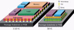
- 3D ICs require fundamentally new ESD verification strategies. Traditional 2D approaches cannot address the complexity and unique connections in stacked-die architectures.
- Classifying external and internal IOs is essential for robust and cost-efficient ESD protection. Proper differentiation
…
Read More
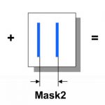
You can’t have failed to notice that 20nm is coming. There are a huge number of things that are different about 20nm from 28nm, but far and away the biggest is the need for double patterning. You probably know what this is by now, but just in case, here is a quick summary.
Lithography is done using 193nm light. Today we use immersion… Read More