You are currently viewing SemiWiki as a guest which gives you limited access to the site. To view blog comments and experience other SemiWiki features you must be a registered member. Registration is fast, simple, and absolutely free so please,
join our community today!
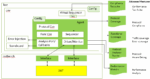
In the rapidly evolving landscape of semiconductor manufacturing, the demand for processors that handle increasing workloads while maintaining power efficiency and compact form factors has never been higher. Intel’s Foveros 2.5D packaging technology emerges as a pivotal innovation, enabling denser die integration… Read More
By Ujjwal Negi – Siemens EDA
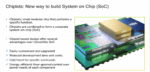
Multi-die architectures are redefining the limits of chip performance and scalability through the integration of multiple dies into a single package to deliver unprecedented computing power, flexibility, and efficiency. At the heart of this transformation is the Universal Chiplet Interconnect… Read More
Today Alchip Technologies, a Taipei-based leader in high-performance and AI computing ASICs, announced a significant milestone with the successful tape-out of its 3D IC test chip. This achievement not only validates Alchip’s advanced 3D IC ecosystem but also positions the company as a frontrunner in the rapidly evolving field… Read More
The rapid evolution of artificial intelligence (AI) is transforming industries, from autonomous vehicles to data centers, demanding unprecedented computational power and efficiency. As highlighted in Synopsys’ guide, the global AI chip market is projected to reach $383 billion by 2032, growing at a 38% CAGR. This … Read More
In an era dominated by artificial intelligence (AI), machine learning (ML), and high-performance computing (HPC), the demand for semiconductors that deliver high data throughput, low latency, and energy efficiency has never been greater. Traditional chip designs often struggle to keep pace with these requirements, leading… Read More
As multi-die and chiplet-based system designs become more prevalent in advanced electronics, much of the focus has been on physical design challenges. However, verification—particularly functional correctness and interoperability of inter-die connections—is just as critical. Interfaces such as UCIe or custom interconnects… Read More
The Universal Chiplet Interconnect Express (UCIe) 3.0 specification marks a decisive step in the industry’s shift from monolithic SoCs to modular, multi-die systems. Released on August 5, 2025, the new standard doubles peak link speed from 32 GT/s in UCIe 2.0 to 48 and 64 GT/s while adding a suite of manageability and efficiency
…
Read More
AI’s exponential growth is transforming semiconductor design—and memory is now as critical as compute. Multi-die architecture has emerged as the new frontier, and custom High Bandwidth Memory (cHBM) is fast becoming a cornerstone in this evolution. In a panel session at the Synopsys Executive Forum, leaders from AWS, Marvell,… Read More
The explosion of artificial intelligence (AI) is transforming the data center landscape, pushing the boundaries of compute, connectivity, and memory technologies. The exponential growth in AI workloads—training large language models (LLMs), deploying real-time inference, and scaling distributed applications—has … Read More
Intel, long a leader in semiconductor manufacturing, is on a determined journey to reclaim its technological leadership in the industry. After facing significant challenges in recent years, the company is making a concerted effort to adapt and innovate, with a clear focus on AI-driven technologies, advanced packaging solutions,… Read More