I recently had the pleasure of attending the AI Hardware Summit at the Computer History Museum in Mountain View, CA. This two-day conference brought together many companies involved in building artificial intelligence solutions. Though the focus was on building the hardware for this area, there was naturally much discussion… Read More
Tag: stacked die
2.5D supply chain takes HBM over the wall
SoC designers have hit the memory wall head on. Although most SoCs address a relatively small memory capacity compared with PC and server chips, memory power consumption and bandwidth are struggling to keep up with processing and content expectations. A recent webinar looks at HBM as a possible solution.… Read More
Testing, testing… 3D ICs
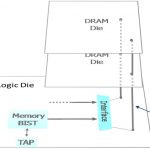
3D ICs complicate silicon testing, but solutions exist now to many of the key challenges. – by Stephen Pateras
The next phase of semiconductor designs will see the adoption of 3D IC packages, vertical stacks of multiple bare die connected directly though the silicon. Through-silicon vias (TSV) result in shorter and thinner… Read More


