You are currently viewing SemiWiki as a guest which gives you limited access to the site. To view blog comments and experience other SemiWiki features you must be a registered member. Registration is fast, simple, and absolutely free so please,
join our community today!
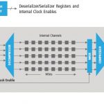
Introducing on-chip test circuitry has become a necessary criteria for an ASIC’s post manufacture testability. The test circuitry is usually referred as DFT (Design-for-Test) circuit. A typical methodology for introducing DFT circuit in a design is to replace usual flip-flops with special types of flip-flops called ‘scan… Read More
With advancement of semiconductor technologies, ever increasing sizes of SoCs bank on higher densities of design rather than giving any leeway towards increasing chip area and package sizes; a phenomenon often overlooked. The result is – larger designs with lesser number of pins bonded out of ever shrinking package sizes;… Read More
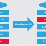
Yesterday Cadence had their annual front-end summit, the theme of which was physically aware design. I was especially interested in the first couple of presentations about physically aware synthesis. I joined Cadence in 1999 when they acquired Ambit Design Systems. One of the products that we had in development was called PKS… Read More