You are currently viewing SemiWiki as a guest which gives you limited access to the site. To view blog comments and experience other SemiWiki features you must be a registered member. Registration is fast, simple, and absolutely free so please,
join our community today!
This article concludes the three-part series examining key methodologies required for successful multi-die design. The first article Reducing Risk Early: Multi-Die Design Feasibility Exploration focused on feasibility exploration and early architectural validation, while the second article Building the Interconnect… Read More
As semiconductor manufacturing pushes deeper into the nanometer regime, computational lithography has evolved from a supporting step into a central pillar of advanced chip design. Mask synthesis, lithography simulation, and optical proximity correction (OPC) now demand unprecedented levels of accuracy and computational… Read More
Semiconductor manufacturing is among the most complex industrial activities in existence. As device geometries shrink and systems become more interconnected, software has become as critical as process technology itself. Modern fabs depend on extensive automation, real-time analytics, and deep integration between tools,… Read More
The semiconductor industry is entering a new era in system design. As traditional monolithic scaling approaches its economic and physical limits, multi-die architectures are emerging as a primary pathway for delivering continued improvements in performance, power efficiency, and integration density. By distributing … Read More
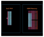
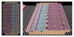
The first article in this series examined how feasibility exploration enables architects to evaluate multi-die system configurations while minimizing early design risk. Once architectural decisions are validated, designers must translate conceptual connectivity requirements into physical interconnect infrastructure.… Read More
As computing expands from data centers to edge devices, semiconductor designers face increasing pressure to optimize both performance and energy efficiency. Advanced process nodes continue to provide transistor-level improvements, but scaling alone cannot meet the demands of hyperscale AI infrastructure or ultra-low-power… Read More
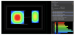
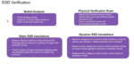
As analog and mixed-signal designs become increasingly complex, parasitic effects dominate both design time and cost, consuming 30–50% of engineers’ effort in debugging and reanalyzing circuits. Addressing these multiphysics effects requires early verification strategies and reliable simulation solutions. Modern … Read More
For more than a decade, progress in artificial intelligence has been framed almost entirely through the lens of compute. Faster GPUs, denser accelerators, and higher TOPS defined each new generation. But as generative and agentic AI enter their next phase, that framing is no longer sufficient. The most advanced AI systems today… Read More
The semiconductor industry is on track to exceed one trillion dollars in annual revenue by the end of the decade, propelled by AI, advanced computing, and edge applications. Yet beneath this growth lies a structural shift. Manufacturing complexity is rising faster than the industry’s ability to manage it. As architectures move… Read More
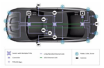
Physical AI is changing how intelligent systems interact with the real world. These systems must sense, process, and respond to data in real time. Unlike cloud AI, Physical AI depends on fast local processing and reliable distributed communication. This shift creates a new challenge. Systems must move large volumes of sensor… Read More