You are currently viewing SemiWiki as a guest which gives you limited access to the site. To view blog comments and experience other SemiWiki features you must be a registered member. Registration is fast, simple, and absolutely free so please,
join our community today!
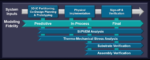
An earlier blog started with the topic of delivering 3D IC innovations faster. The blog covered the following foundational enablers for successful heterogeneous 3D IC implementation.
- System Co-Optimization (STCO) approach
- Transition from design-based to systems-based optimization
- Expanding the supply chain and tool
…
Read More
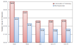
Discussions of chiplets has been on the rise, ever since the slowdown of Moore’s law benefits. Gartner Research projects semiconductor revenue from systems using chiplets to grow from $3.3 billion in 2020, to $50.5 billion in 2024. With any market opportunity, there are always challenges to overcome in order to realize the full… Read More
Over the recent years, the volume and velocity of discussions relating to chiplets have intensified. A major reason for this is the projected market opportunity. According to research firm Omdia, chiplets driven market is expected to be $6B by 2024 from just $645M in 2018. That’s an impressive nine-fold projected increase over… Read More