DAC 2026by Admin on 01-07-2026 at 3:05 am
The Long Beach Convention Center will serve as a dynamic venue for DAC 2026: The Chips to Systems Conference. Set along the scenic Southern California coastline, the center offers modern meeting spaces and a vibrant setting that reflects the innovative spirit of DAC. Its central location in downtown Long Beach provides easy access… Read More
Join us for the User2User North America event, which is a dedicated environment for exchanging ideas, information and best practices that enable you to lead in your role and achieve success with your customers.
About User2User
User2User is your opportunity to learn, grow and connect with fellow technical experts… Read More
William Wang is a world-leading expert in artificial intelligence, specializing in generative AI and large language models. As the Founder, CEO, and Chairman of Alpha Design AI, he brings a wealth of experience from academia and industry, having previously shipped Amazon Q at Amazon AWS Bedrock
A Mellichamp Chair Professor … Read More
By Jason Liu, RFIC-GPT Inc.
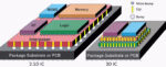
Radio frequency integrated circuits (RFICs) have become increasingly critical in modern electronic systems, driven by the rapid growth of wireless communication technologies (5G/6G), the Internet of Things (IoT), and advanced radar systems. With the desire for lower power consumption, higher… Read More
In the fast-evolving world of electronic design automation (EDA), where complexity multiplies with every nanometer shrink and AI integration, data silos are the silent killers of innovation. Keysight Technologies, a leader in design and test solutions, tackles this head-on with their webinar “From Silos to Systems,… Read More
By Niranjan Sitapure
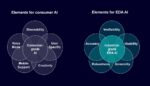
Artificial intelligence (AI) is reshaping industries worldwide. Consumer-grade AI solutions are getting significant attention in the media for their creativity, speed, and accessibility—from ChatGPT and Meta’s AI app to Gemini for image creation, Sora for video, Sona for music, and Perplexity for web… Read More
Murat Eskiyerli, PhD, is the founder of Revolution EDA
Modern software development environments have evolved dramatically. A developer can download Visual Studio Code, install a few plugins, and be productive within minutes. The cost? Perhaps a few hundred dollars per month for cloud development resources. Compare that to… Read More
By Liyue Yan (lyan1@bu.edu)
Fact 1: In the Computer History Museum, how many artifacts are about Electronic Design Automation (EDA)? Zero.
Fact 2: The average starting base salary for a software engineer at Netflix is $219K, and that number is $125K for Cadence; the starting base salary for a hardware engineer at Cadence is $119K… Read More
By Kamal Khan
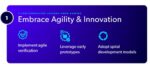
The semiconductor world has always been the beating heart of tech innovation, powering everything from our smartphones to the latest AI breakthroughs. However, as chip complexity increases and market demands accelerate, adherence to traditional development cycles may be stagnating design teams and slowing … Read More