You are currently viewing SemiWiki as a guest which gives you limited access to the site. To view blog comments and experience other SemiWiki features you must be a registered member. Registration is fast, simple, and absolutely free so please,
join our community today!
By Kamal Khan
The semiconductor world has always been the beating heart of tech innovation, powering everything from our smartphones to the latest AI breakthroughs. However, as chip complexity increases and market demands accelerate, adherence to traditional development cycles may be stagnating design teams and slowing … Read More
Today, Perforce IPLM stands at the intersection of data management, automation, and collaboration, shaping the way companies design the next generation of chips and systems. Looking ahead, its evolution will reflect the growing convergence of hardware, software, and AI-driven engineering.
WEBINAR – Future Forward:… Read More
By Omar Elabd
As semiconductor designs move below 7 nm, parasitic effects—resistance, capacitance and inductance—become major threats to IC performance and reliability, often hiding where netlist reviews cannot reach. Design teams need advanced visualization tools like heat maps, layer-based analysis and direct layout… Read More
By Mark Tawfik
Overview: Protecting ICs from costly ESD and latch-up failures
Electrostatic discharge (ESD) events cost the semiconductor industry an estimated $8 billion annually in lost productivity, warranty claims and product failures [1].
Ensuring the robust protection of integrated circuits (ICs) against various… Read More
By Zameer Mohammed
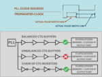
This article claims to provide clear key insights of Min Pulse Width (MPW) timing signoff check, proactive closure strategies for faster time-to-market, and effective methods to prevent silicon failures.
Min Pulse Width (MPW) check for timing signoff has become an important design constraint at the sub-5nm… Read More
DATE 2026by Admin on 08-27-2025 at 10:57 pm
Design, Automation and Test in Europe Conference |
The European Event for Electronic System Design & Test
The DATE conference is the main European event bringing together designers and design automation users, researchers and vendors, as well as specialists in hardware and software design, test, and manufacturing
…
Read More
On July 9, 2025, a DACtv session featured a Google product manager discussing the strategic importance of electronic design automation (EDA) and how Google Cloud is optimizing it for the semiconductor industry, as presented in the YouTube video. The talk highlighted Google Cloud’s role in addressing the escalating complexity… Read More
On July 9, 2025, Derren Dunn from IBM Research’s TJ Watson Research Center delivered a DACtv presentation, as seen in the YouTube video detailing IBM’s EDA-as-a-Solution platform. This innovative offering leverages IBM’s high-performance computing (HPC) cloud to deliver hybrid and cloud-only infrastructure for electronic… Read More
On July 9, 2025, a DACtv session by Dr. Peter Levin explored the transformative impact of artificial intelligence (AI) on chip design, as presented in the YouTube video. The speaker, an industry expert, delved into how AI is reshaping electronic design automation (EDA), addressing the escalating complexity of modern chips and… Read More
Probably one of the most anticipated semiconductor investor calls was held last week and it did not disappoint. It was Lip-Bu Tan’s first full quarter since he took over as CEO. In the resulting discussions on the SemiWiki Forum I am viewed as overly optimistic of Intel’s recent pivot. That is true, I am optimistic, but my observations… Read More


![[white paper] Parasitic Analysis Figures](https://semiwiki.com/wp-content/uploads/2025/10/Fig1-net-level-visualization-150x127.jpg)