You are currently viewing SemiWiki as a guest which gives you limited access to the site. To view blog comments and experience other SemiWiki features you must be a registered member. Registration is fast, simple, and absolutely free so please,
join our community today!
The second segment of Oski’s most recent “Decoding Formal” event was a talk by Anatoli Sokhatski (formal tech lead at Cisco) on training and methodology development for a structured and scalable approach to formal verification, particularly with emphasis on formal signoff.
Anatoli stressed that he and others in the team did … Read More
I think by now a lot has been said about the necessity of multi-patterning at advanced technology nodes with extremely low feature size such as 20nm, because lithography using 193nm wavelength of light makes printing and manufacturing of semiconductor design very difficult. The multi-patterning is a novel semiconductor manufacturing… Read More
Diagnosing Double Patterning Violationsby Beth Martin on 10-28-2013 at 5:16 pmCategories: EDA, Siemens EDA
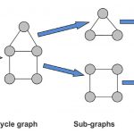
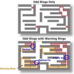
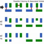
I’ll bet you’ve read a bunch of stuff about double patterning, and you’re probably hoping that the design tools will make all your double patterning issues just go away. Well, the truth is that the foundries and EDA vendors have worked really hard to make that true.
However, for some critical portions of your design, there … Read More
David Avercrombie of Mentor won the award for the best tutorial at the 2012 TSMC OIP for his presentation, along with Peter Hsu of TSMC, on Finding and Fixing Double Patterning Errors in 20nm. The whole presentation along with the slides is now available online here. The first part of the presentation is an introduction to double … Read More
You can’t have failed to notice that 20nm is coming. There are a huge number of things that are different about 20nm from 28nm, but far and away the biggest is the need for double patterning. You probably know what this is by now, but just in case, here is a quick summary.
Lithography is done using 193nm light. Today we use immersion… Read More


