You are currently viewing SemiWiki as a guest which gives you limited access to the site. To view blog comments and experience other SemiWiki features you must be a registered member. Registration is fast, simple, and absolutely free so please,
join our community today!
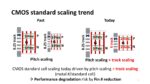
In the rapidly evolving semiconductor landscape, imec’s recent breakthroughs in wafer-to-wafer hybrid bonding and backside technologies are reshaping the future of compute systems. As detailed in their article, these innovations transition CMOS 2.0 from a conceptual framework to practical reality, enabling denser,… Read More
At IEDM 2023, Naoto Horiguchi presented on CFETs and Middle of Line integration. I had a chance to speak with Naoto about this work and this write up is based on his presentation at IEDM and our follow up discussion. I always enjoy talking to Naoto, he is one of the leaders in logic technology development, explains the technology in … Read More