You are currently viewing SemiWiki as a guest which gives you limited access to the site. To view blog comments and experience other SemiWiki features you must be a registered member. Registration is fast, simple, and absolutely free so please,
join our community today!
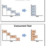
I will address this topic with two blog posts: validation (i.e. post silicon) — Part 1, and verification (pre-silicon) — Part 2 (coming soon!). In this blog post, I will focus on validation.
One of the upsides of using catalog chips that have been in the market for a long time and have ramped in substantial volumes is that… Read More
Every SoC project that I know of wants to finish on time, under budget, and maximize profits per device. When I first started out doing DRAM design I learned that we could maximize profit by doing shrinks of existing designs, move from ceramic to plastic packages, and reduce the amount of time spent on a tester. Today, the economic … Read More
With advancement of semiconductor technologies, ever increasing sizes of SoCs bank on higher densities of design rather than giving any leeway towards increasing chip area and package sizes; a phenomenon often overlooked. The result is – larger designs with lesser number of pins bonded out of ever shrinking package sizes;… Read More


