Each year on the Sunday before the SPIE Advanced Lithography Conference, Nikon holds their LithoVision event. This year I had the privilege of being invited to speak for the third consecutive year, unfortunately, the event had to be canceled due to concerns over the COVID-19 virus but by the time the event was canceled I had already… Read More
Tag: 3.5nm
LithoVision 2018 The Evolving Semiconductor Technology Landscape and What it Means for Lithography
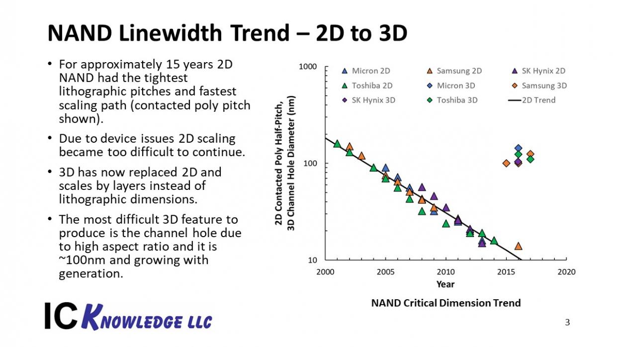
I was invited to present at Nikon’s LithoVision event held the day before the SPIE Advanced Lithography Conference in San Jose. The following is a write up of the talk I gave. In this talk I discuss the three main segments in the semiconductor industry, NAND, DRAM and Logic and how technology transitions will affect lithography.… Read More
Scott Jones ISS Talk – Moore’s Law Lives!
I was invited to give a talk at this year’s ISS conference, the talk seemed to be very well received and I was asked to blog about it for SemiWiki. Parts of the talk will be familiar to SemiWiki readers from some of my previous blogs but I also went into more detail around some scaling challenges. The following is a summary of what… Read More


