You are currently viewing SemiWiki as a guest which gives you limited access to the site. To view blog comments and experience other SemiWiki features you must be a registered member. Registration is fast, simple, and absolutely free so please,
join our community today!
One of my favorite classes in college was the lab exercise, mostly because we actually got to use real electronics and then measure something, finally writing it up in our lab notebooks. The issue today is that a college student taking Electrical Engineering probably doesn’t have much access to 10nm FinFET silicon for use… Read More
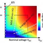
User group meetings are a rich source of information for IC designers because they have actual designers talking about how they used EDA tools in their methodology to achieve a goal. Engineers at STMicroelectronicspresented at a MunEDAUser Group on the topic: I/O Design Optimization Flow For Reliability In Advanced CMOS Nodes.… Read More