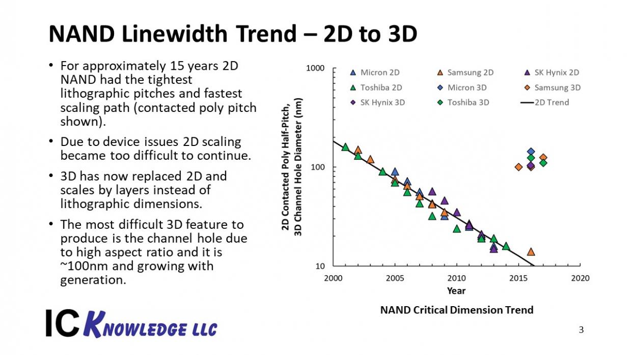
I was invited to present at Nikon’s LithoVision event held the day before the SPIE Advanced Lithography Conference in San Jose. The following is a write up of the talk I gave. In this talk I discuss the three main segments in the semiconductor industry, NAND, DRAM and Logic and how technology transitions will affect lithography.… Read More


