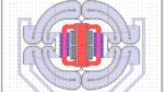
The semiconductor industry is experiencing rapid evolution, driven by the proliferation of IoT applications, image sensors, photonics, MEMS applications, 3DIC and other emerging technologies. This growth has dramatically increased the complexity of integrated circuit (IC) design. One aspect of this complexity is the … Read More
The ASIC business has always been a key enabler of the semiconductor industry but it is a difficult business. In my 40 years I have seen many ASIC companies come and go but I have never seen one like Alchip.
Alchip Technologies Ltd. was founded more than 20 years ago, about half way through my career. I know one of the founders, a fiercely… Read More
You could be forgiven for thinking of hearing aids as the low end of tech, targeted to a relatively small and elderly audience. Commercials seem unaware of advances in mobile consumer audio, and white-haired actors reinforce the intended audience. On the other hand, the World Health Organization has determined that at least 6%… Read More
Dan is joined by Christopher Vick, the Vice President of Engineering at Lemurian Labs, bringing over three decades of experience from top tech companies such as Qualcomm, Oracle, and Sun Microsystems. Throughout his distinguished career, Christopher has played a key role in developing technologies used by billions.
Notably,… Read More
Tobias began his journey with a strong academic foundation in electronic design automation, studying at a leading university in Germany that specialized in formal verification. After graduating, Tobias gained hands-on experience in the semiconductor industry, where he quickly recognized the challenges and inefficiencies… Read More
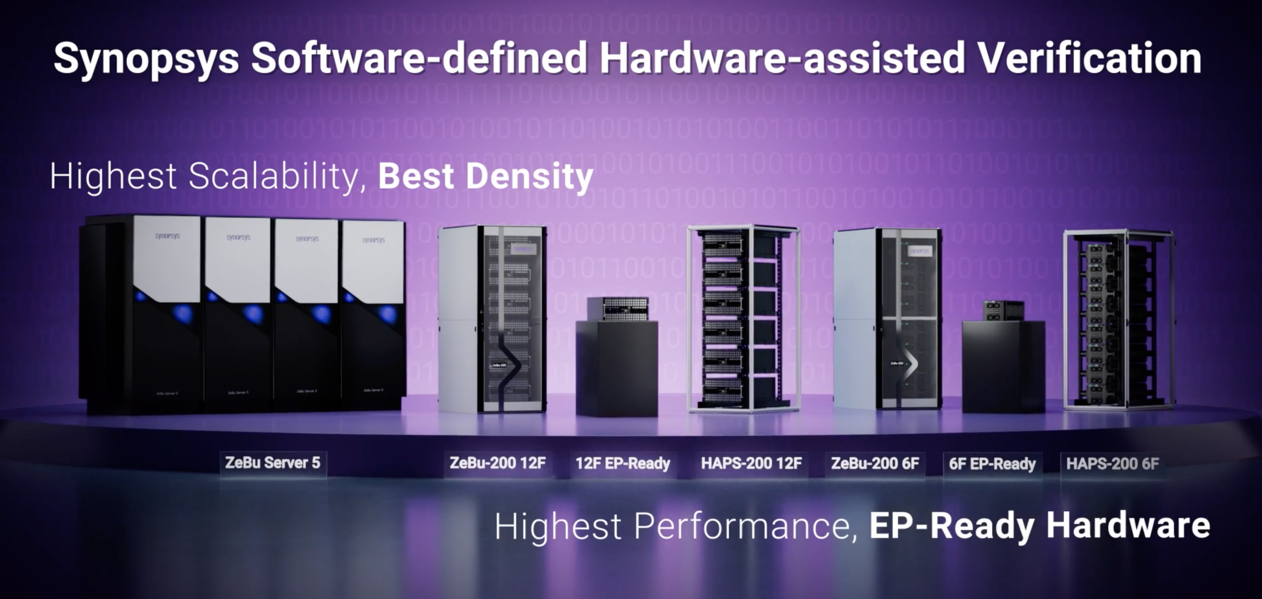
Artificial intelligence (AI) is driving a transformation in data center infrastructure, necessitating cutting-edge technologies to meet the growing demands of AI workloads. As AI systems scale up and out, next-gen compute servers, switches, optical-electrical links, and flexible, redundant networking solutions are … Read More
If the thought of a silicon respin keeps you awake at night, you’re not alone. Re-fabricating a chip can cost tens of millions of dollars. An unplanned respin also risks a delay in getting a product to market, which adds tremendous costs in terms of lost business.
Undoubtedly, adding to your sleep loss is the recent rise in respins.… Read More
Many of you are already familiar with Silicon Catalyst and the value it brings to semiconductor startups, the industry and the electronics industry at large. Silicon Catalyst is an organization that supports early-stage semiconductor startups with an ecosystem that provides tools and resources needed to design, create, and… Read More
Silicon Carbide (SiC) is the superhero EV converters need, boosting efficiency, shrinking component sizes, and letting your car charge faster while handling heat like a pro. Even Tesla’s like, “Yep, we’re using it,” because who doesn’t want more range and less sweating under the hood?
By Jerome Fohet
Get ready for… Read More
At the 2024 TSMC OIP Ecosystem Forum, one of the technical talks by TSMC focused on maximizing 3DIC design productivity and rightfully so. With rapid advancements in semiconductor technology, 3DICs have become the next frontier in improving chip performance, energy efficiency, and density. TSMC’s focus on streamlining the… Read More


Musk’s Orbital Compute Vision: TERAFAB and the End of the Terrestrial Data Center