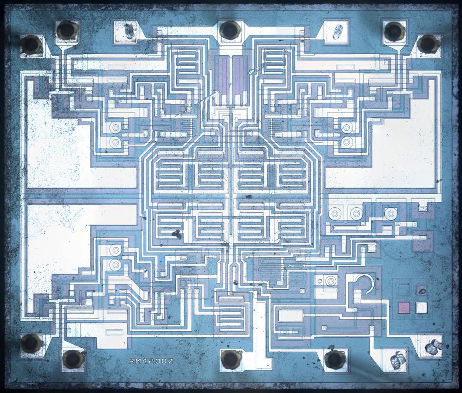
A recent Twitter thread about a counterfeit analog multiplier chip attracted my attention since I’m interested in both counterfeit integrated circuits and how analog computers multiply. In the thread, John McMaster decapped a suspicious AD633 analog multiplier chip and found an entirely different Rockwell RC4200 die inside. Why would someone do this? Probably because the RC4200 (1978) currently sells for about 85 cents, while the more modern laser-trimmed1 AD633 (1989) sells for about $7.2
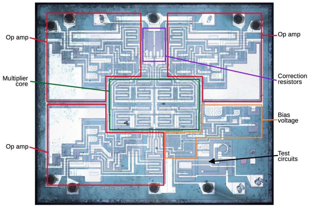
Analog multiplication
Analog multiplication has many uses such as mixers, modulators, and phase detectors, but analog computers are how I encountered analog multiplication. A typical analog computer uses voltages to represent values and is wired up through a plugboard to solve a particular equation. Adding or subtracting two values is easy with an op amp, as is multiplying by a constant. Integration seems like it would be difficult, but it’s almost trivial with a capacitor; analog computers excelled at solving differential equations.
Multiplying two values, however, was surprisingly difficult; multiplication techniques were slow, inaccurate, noisy, or expensive. One accurate but slow multiplier used the Rube-Goldberg configuration of servo motors turning potentiometers.3 A 1969 multiplier circuit uses a light bulb and photocells. A fast and accurate approach was the “parabolic multiplier”, built from numerous expensive high-precision resistors.4 The approach I’ll discuss is to multiply by adding the logarithms and taking the exponential. Inconveniently, this approach magnifies even small differences between the transistors. It is also very sensitive to temperature. As a result, this approach was simple but inaccurate.
However, the development of analog integrated circuits created new opportunities for analog multiplication circuits. In particular, since the transistors in an integrated circuit were created together, they have nearly-identical properties. And the components on a tiny silicon die are all at nearly the same temperature.5
The first analog multiplier integrated circuit I could find is a television demodulator from 1967. The Gilbert cell technique was introduced by Barrie Gilbert in 1968 and is used in most analog multipliers today.6 The AD530 was introduced around 1970, and became an industry standard, but required external adjustments for accuracy. Laser-trimming the resistors inside the integrated circuit during manufacturing greatly improved the accuracy, an approach used in the AD633, the integrated circuit that was counterfeited.
Before explaining the circuitry of the RC4200 (the multiplier inside the counterfeit chip), I’ll discuss the components that it is constructed from, and how they appear in an integrated circuit. This will help you recognize these structures in the die photo.
Transistors
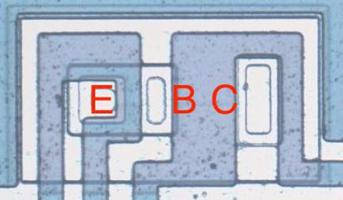
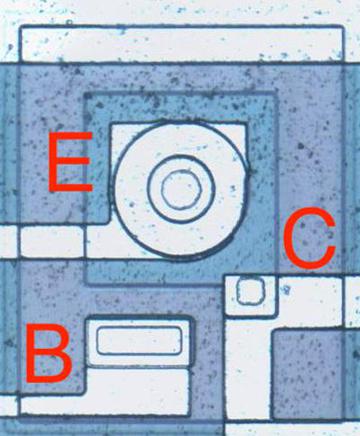
Transistors are the key components in a chip. The photo below shows an NPN transistor in the RC4200 as it appears on the chip. The different blue colors are regions of silicon that have been doped differently, forming N and P regions. The white lines are the metal layer of the chip on top of the silicon—these form the wires connecting to the emitter (E), base (B), and collector (C).
You might expect PNP transistors to be similar to NPN transistors, just swapping the roles of N and P silicon. But for a variety of reasons, PNP transistors have an entirely different construction. They consist of a circular emitter (P), surrounded by a ring-shaped base (N), which is surrounded by the collector (P). This forms a P-N-P sandwich horizontally (laterally), unlike the vertical structure of the NPN transistors. The diagram below shows one of the PNP transistors in the RC4200.
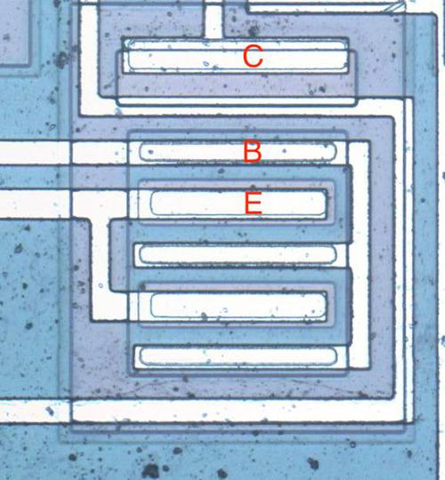
The input and output transistors in the RC4200 are larger than the other transistors and have a different structure to support higher currents. The photo below shows one of the output transistors. Note the multiple interdigitated “fingers” of the emitter and base.
Capacitors
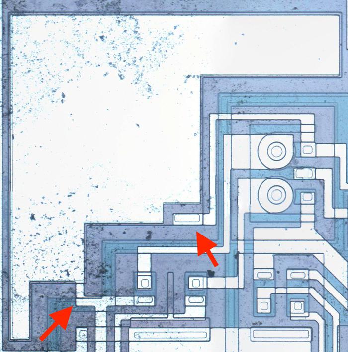
Capacitors are important in op amps to provide stability. A capacitor can be built in an integrated circuit as a large metal plate separated from the silicon by an insulating oxide layer. The main drawback of capacitors on ICs is they are physically very large. The 15pF capacitors in the RC4200 have a very small capacitance but take up a large fraction of the die area. In the photo below, the red arrows indicate the connection to the capacitor’s metal layer and to the capacitor’s underlying silicon layer.
Resistors
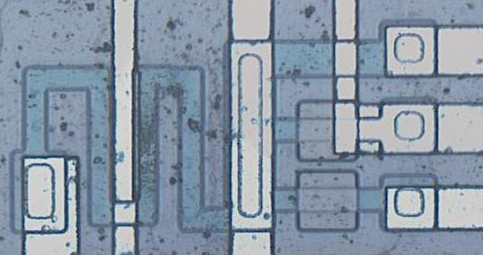
Resistors are a key component of analog chips. Unfortunately, resistors in ICs are very inaccurate; the resistances can vary by 50% from chip to chip. The photo below shows four resistors, formed using different techniques. The first resistor is the zig-zagging blue region on the left. It is formed from a strip of P silicon, with metal wiring (white) attached on the left and right. Its resistance is 3320 Ω. The resistor in the upper right is much shorter, so it is only 511Ω (long, narrow resistors have higher resistance than short, wide resistors). The remaining resistors are 20KΩ despite their small size because they are “pinch resistors”. In the pinch resistor, the square layer of brownish N silicon on top makes the conductive region much thinner (i.e. pinches it). This allows a much higher resistance for a given size. (Otherwise, a 20 KΩ resistor would be 6 times as long as the first resistor, taking up excessive space.) The tradeoff is the pinch resistor is much less accurate.
Multiplying with logs and exponentials
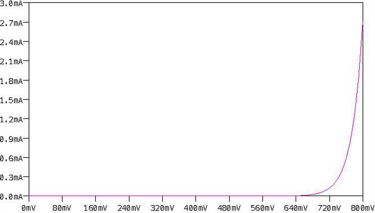
This integrated circuit multiplies using the log-antilog technique. The idea is that if you take the log of two numbers, add the logs together, and then take the antilog (i.e. exponential), you get the product of the two numbers. Conveniently, transistors have a logarithmic / exponential characteristic: the current through the transistor is an exponential of the voltage on the base. Specifically, if VBE is the voltage between the transistor’s base and emitter, the current through the collector (IC) is an exponential of that voltage, as shown in the graph below. The analog multiplier takes advantage of this property.
The main complication with this approach is that the curve above is very sensitive to the temperature and to the manufacturing characteristics of the transistor. Because the curve is exponential, even a small shift in the curve will radically change the current. This was a serious difficulty when building a multiplier from discrete transistors, since the properties varied from transistor to transistor. To stabilize the temperature, some multipliers used a temperature-controlled oven. However, using an integrated circuit mostly solved these problems. The transistors in an integrated circuit are well-matched since they were built from the same piece of silicon under the same conditions. And the transistors in an integrated circuit die will be at almost the same temperature. Thus, integrated circuits made transistor-log circuits much more practical.
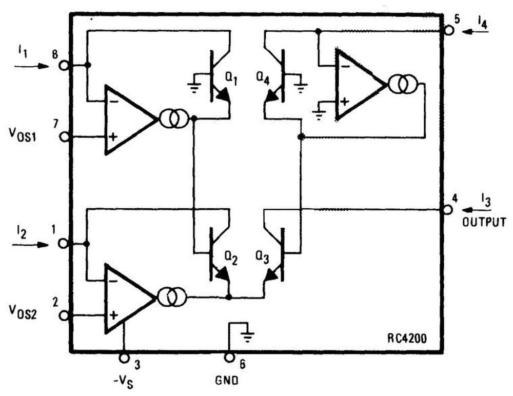
The diagram below shows the structure of the RC4200 multiplier chip. The user provides three current inputs (I1, I2, and I4) and the chip computes the output current I3, where I3 = I1×I2÷I4. (The use of current inputs and outputs is a bit inconvenient compared to other multipliers, such as the AD633, that use voltages.)
The four transistors in the middle of the diagram are the multiplier core, the key to the IC’s operation. The transistors are configured so their base-emitter voltages sum: VBE3 = VBE1+VBE2-VBE4. Because the transistor current is related exponentially to the voltage, the result is that I3 = I1×I2÷I4.
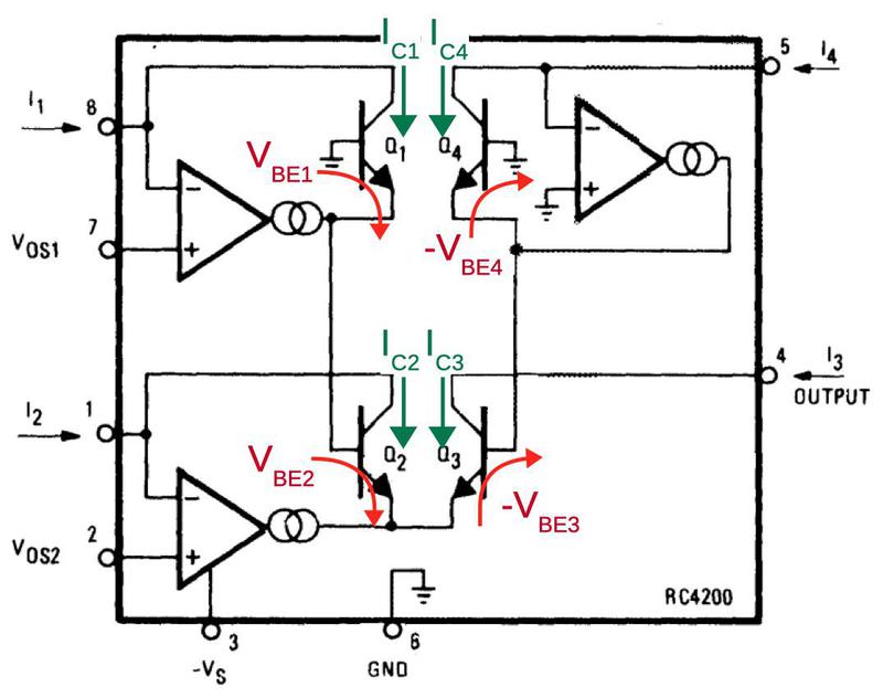
In more detail, first note that the voltages VBE1 through VBE4 control the collector currents IC1 through IC4 through the transistors (below). The op amps adjust the base-emitter voltages so the input currents match the transistor currents, i.e. I1 = IC1 and so forth. (This is accomplished by op amp feedback.) Now, if you go through the loop of base-emitter voltages starting at the base of Q1 and ending at the base of Q4 (red arrows), you find that VBE1+VBE2-VBE3-VBE4 = 0. (The voltages must sum to zero since you start at ground and end at ground.7) Now, because IC is related to exp(VBE), taking the exponential of the equation yields IC1×IC2÷IC3÷IC4 = 1. (Details in footnote8.)
Next, I’ll explain how the VBE voltages are generated. Each current input has an op amp associated with it that produces the “correct” VBE voltage for the current using a feedback loop9 For example, suppose IC is too low so not all the input current flows through the transistor. The excess current will raise the voltage on the op amp’s negative input, causing it to reduce its output voltage and thus the transistor’s emitter voltage. This raises VBE (since the base will now be higher compared to the emitter), causing more collector current to flow through the transistor. Similarly, if too much current is flowing through the transistor, the op amp’s input will be pulled lower, reducing VBE. Thus, the feedback loop causes the op amp to find the exact VBE for the current input.10
Correcting for emitter resistance
The above circuit works reasonably well, but there’s a complication: the transistors have a small emitter resistance R. The voltage drop across this resistance will increase VBE by ICR, disturbing the nice exponential behavior. This creates a nonlinearity that reduces the accuracy of the result. The datasheet says that “Raytheon has developed a unique and proprietary means of inherently compensating for this undesired term.” They don’t explain this further, but by studying the die I have figured out how it works.
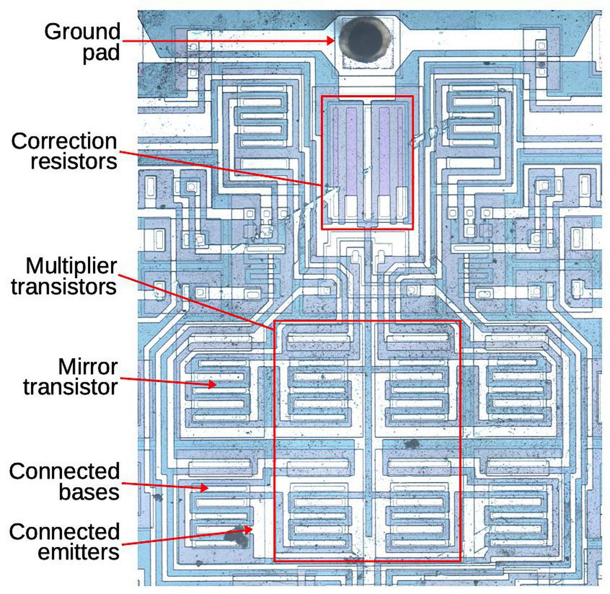
In the compensation circuit, each of the four multiplier transistors is paired with an identical “mirror” transistor with the corresponding emitters and corresponding bases connected, as shown below. These connections give the paired transistors the same base and emitter voltages, so they have the same collector currents. In other words, they form a current mirror. The mirrored currents are fed into special correction resistors that match the undesired emitter resistance, 0.1 Ω according to the datasheet.11 The voltage across the correction resistors will be the same as the excess voltage that needs to be compensated (since the resistance and current are the same). The final step is the correction resistors are connected to the base of the multiplication transistors, replacing the connection to ground. This will shrink VBE by the amount it was erroneously increased, fixing the computation.
Why are there two correction resistors? Recall that the multiplier has two transistors adding and two transistors subtracting (i.e. VBE1+VBE2-VBE3-VBE4 = 0). To handle this, the correction circuit is split in two. The left half sums IC1 and IC2 and applies this current to a correction resistor on the Q3/Q4 side, while the right half sums IC3 and IC4 and applies this to a correction resistor on the Q1/Q2 side. The addition and subtraction work out to yield the desired net correction.
Schematic
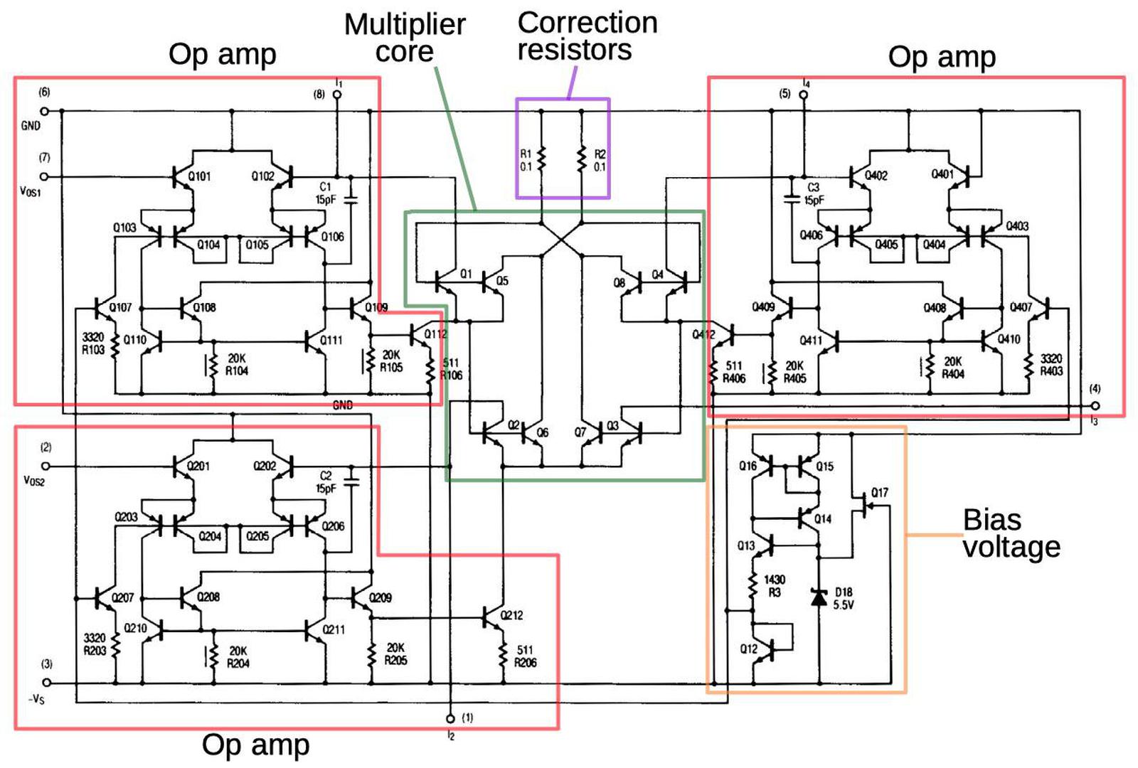
The schematic below shows the complete circuitry of the RC4200; I’ve highlighted the main functional blocks. (Inconveniently, I didn’t find this schematic until after I’d traced out the circuitry from the die photo.) The multiplier core and the correction resistors were discussed above The op amps circuits are fairly similar to the 741 op amp, which I’ve written about. They lack the output stage of typical op amps; the output transistor (Q112/Q212/Q412) corresponds to the intermediate gain state in a typical op amp. The bias circuit (orange, lower right) provides a fixed bias voltage for the op amps.12
Conclusion
Before integrated circuits, analog multiplication was difficult to implement. However, integrated circuits made it easy to create matched transistors, leading to fast, inexpensive analog multiplication integrated circuits. Unfortunately, analog multiplier integrated circuits were introduced just as analog computers were dying out, killed by inexpensive digital microprocessors, so analog computing missed most of the benefit of these chips.
While most analog multipliers use a circuit called the Gilbert cell, the Raytheon RC4200 analog multiplier uses a different technique to multiply and divide values represented by currents. Although, it includes a special error compensation circuit to improve its accuracy, it is obsolete compared to accurate, laser-trimmed multipliers. Now, counterfeiters re-label RC4200 chips and sell them as the more-expensive AD633 multiplier.
I announce my latest blog posts on Twitter, so follow me at kenshirriff for updates. I also have an RSS feed. Thank you to John McMaster for the die photos used in this blog post; the photos are here.
Notes and references
- One reason that the AD633 multiplier is so expensive is that the resistors on the die are laser-trimmed resistors for accuracy. To get an accurate result, an analog multiplier requires exactly-tuned resistances. The older RC4200 requires adjustable external resistors, which is much less convenient. ↩
- I’m a bit puzzled by this counterfeit chip. Sometimes people will label a cheap op amp as an expensive op amp, as explained by Zeptobars. At first glance, that’s what’s going on here: a cheap multiplier repackaged as an expensive one. However, the two multipilers are so different that I can’t imagine one working at all in place of the other. Specifically, the AD633 takes differential voltage inputs and outputs two currents (a differential current), and it computes A×B+C. The RC4200, on the other hand, takes current inputs and outputs a single current, and it computes A×B÷C. ↩
- An example of a servo multiplier is the Solartron Servo Multiplier from the late 1950s. This 17-pound unit contained a potentiometer controlled by a servo motor, allowing it to multiply numbers represented by +/- 100 volts. It’s surprisingly fast considering its mechanical operation, responding in under 30 milliseconds. Power consumption was high: 70 watts, cooled by a fan. (In comparison, the RC4200 chip uses 40 milliwatts of power.)↩
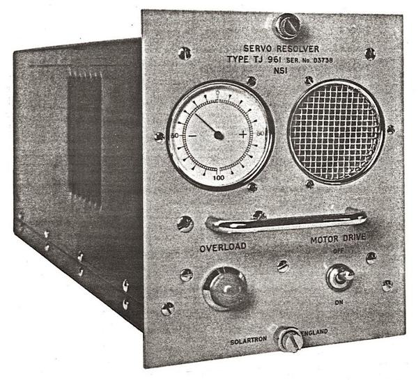 This photo shows the Solartron TJ961 Servo Resolver. This implements multiplication as well as sine/cosine computation. Photo from manual via Analog Museum.
 - The 1969 analog computer I’m restoring uses a parabolic multiplier, a technique used for high-accuracy multiplication. The idea is that to compute A×B, you compute ((A+B)^2 – (A-B)^2)/4, which has the same value. That equation looks much more complex than the original product, but is easier to implement on an analog computer because op amps can perform the sums, subtraction, and division by four. Squaring is easier than multiplication because it is a function of a single variable, so it can be implemented by an “arbitrary function generator”.
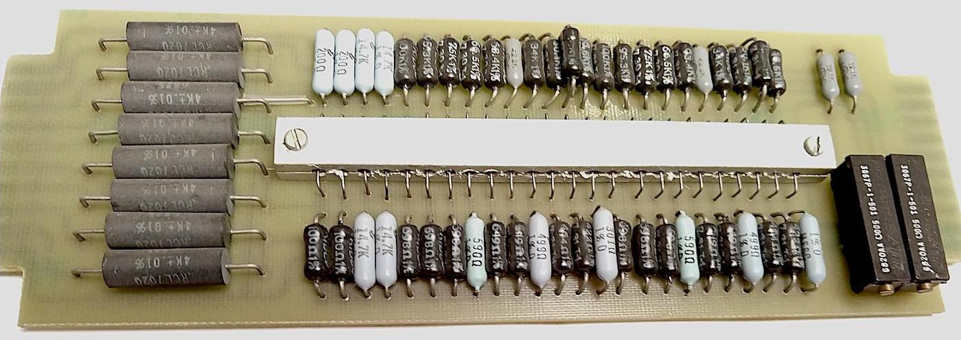 Parabolic multiplier circuit board from a Simulators, Inc. 2400 analog computer.
The photo above shows a function board from an analog computer that computes the square, i.e. a parabola. The board approximates the function by multiple piecewise-linear segments, each defined by resistors. (Note the extremely accurate 0.01% resistors on the left.) The metal block in the center holds diodes, temperature-balanced by the metal. Each diode is biased to turn on at a particular voltage; the diodes act as switches, selecting the appropriate resistors for each linear segment. Note the large amount of precision hardware required for multiplication; a single product requires two of these parabolic function boards as well as multiple op amps. ↩
- To minimize the effect of temperature on the integrated circuit, the critical multiplier transistors are placed close together in the center of the chip. If there is a thermal gradient across the chip, this will minimize the temperature difference between the transistors. (Compared to putting the transistors in the corners, for instance.) To reduce temperature gradients even more, the datasheet specifies a “thermal symmetry line”. Putting a temperature source on this line ensures that the hotter transistors will tend to cancel each other out.↩
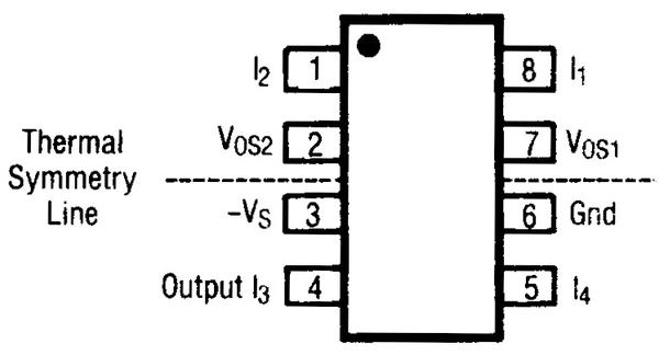 The datasheet shows the IC’s thermal symmetry line.
 - Barrie Gilbert, inventor of the Gilbert cell, has a video explaining translinear circuit, circuits based on the exponential current-voltage relationship of a bipolar transistor. This video explains translinear analog multipliers in detail, discussing two approaches> The first approach, used by the RC4200, is the “log-antilog” approach, where op-amps force and sense the collector currents. The second, used in the AD633 and many other multipliers, is the “integrated” approach, built from voltage-to-current conversion, a differential current-mode core, and current-to-voltage conversion. ↩
- I should mention that the chip uses a -15 V supply, so ground is the highest voltage and the other internal voltages are all negative. Just a warning since this makes things confusing and backward compared to circuits where ground is the low voltage. ↩
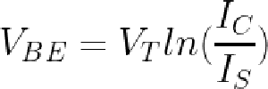
- The relationship between the base voltage and the collector current is given by the Ebers-Moll model. This equation (below) is filled with interesting constants: α: a gain factor (almost 1), k: the Boltzmann constant, IS: the saturation current (extremely small, order of 10-15 A), T: the absolute temperature, q: the charge on the electron. (The temperature in the exponential term reflects the importance of temperature stability for the multiplier.)

Substituting the thermal voltage VT (about 26 mV) for kT/q, making some minor approximations, and taking the log yields:
Substituting that into the multiplier’s VBE loop equation yields
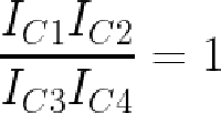
Taking the exponential and assuming the transistors all have the same temperature and saturation current yields the desired equation relating the four currents:
This equation shows how the four currents are related by multiplication and division. See the datasheet for more details. ↩
- In a sense, the op amps compute the inverse of the transistor’s exponential function. The transistor takes VBE as an input and produces the exponential current as an output. However, we have the current as the input and want the logarithmic voltage as the output. By using the op amp with a function in its feedback loop, we can find the inverse of a function, in this case giving us the logarithm. That is, the op amp will converge on the output X where f(X) equals the input, i.e. X = f-1</sup(input). The same technique can be used to generate a square root from a multiplier chip: use the multiplier to square its input, and then use an op amp to compute the inverse function, i.e. the square root. ↩
- You might wonder why the op amp finds the “correct” value and doesn’t overshoot and oscillate. Handwaving away all the theory, the idea is that the capacitor on the op amp input stabilizes it and prevents oscillation. Even so, the datasheet warns that the circuits become unstable as the input currents approach 0. This corresponds to dividing by zero, so it’s not surprising that the circuitry doesn’t handle it well. Mathematically, the op amp is trying to find ln(0), which isn’t going to work. If you want to multiply by zero or negative values, the datasheet describes how the inputs can be biased with resistors to keep the inputs positive but still get the correct answer. ↩
- The two resistors below are used for the emitter correction; they have unusual construction and a very small resistance, 0.1 Ω. Each resistor consists of the two vertical stripes, connected together at the bottom; the vertical region in the center is connected to the ground pin, forming the other side of each resistor. These resistors improve the accuracy of the product by correcting for the emitter resistances. Based on their purple color, which doesn’t appear elsewhere on the die, they appear to be specially doped. The metal contacts at the bottom cover part of the resistor; I believe that by adjusting the size of the metal contacts, the resistor values can be tuned. I believe that the thick and thin regions allow for coarse and fine tuning.
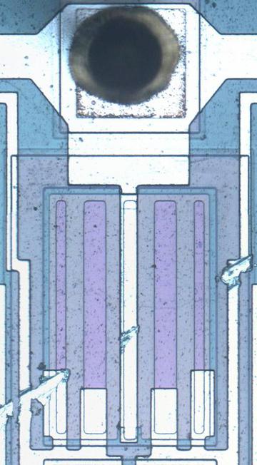 Precise small-valued resistors provide a correction factor.
 - The bias voltage circuit generates a stable voltage of one diode drop (about 800 mV) from Q4’s collector; this voltage biases the op amps. The tricky part is how to keep the power supply voltage from influencing this voltage or the Zener voltage.
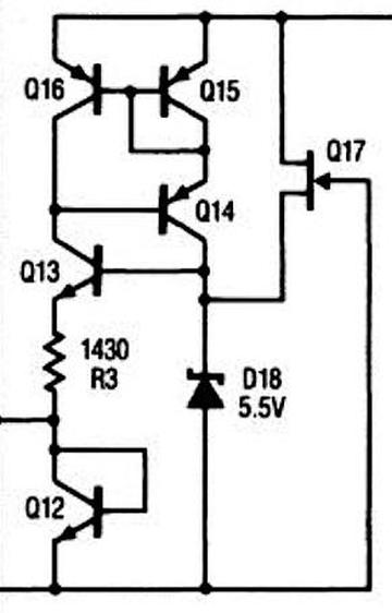 The bias generation circuit, from the datasheet.
The idea is that the Zener diode puts 5.5 volts on the base of Q13. The voltage across R3 will be two diode drops lower (2.8 V) due to Q13 and Q12. This yields a fixed current of 2.8 V / 1430 Ω = 2 mA through Q4, resulting in a stable voltage drop across Q12 and a stable output. But a Zener’s voltage fluctuates a bit with current, so the clever part is how the Zener’s current is kept stable. Transistors Q14, Q15, and Q16 form a current mirror, so the current through the Zener will match the current through the resistor, which is 2 mA. Thus, the Zener voltage keeps the resistor current and output voltage stable, while the resistor current keeps the Zener stable. The final piece of the puzzle is the FET Q17, which provides a tiny current through the Zener to start the feedback cycle. ↩




Silicon Insurance: Why eFPGA is Cheaper Than a Respin — and Why It Matters in the Intel 18A Era