1. A lot of sources indicate that it's harder to stay at high clocks on newer/smaller nodes because of wire resistances, leakage challenges, and thermal density issues that "getting too small" causes.
This is a common misunderstanding. Putting aside the transistor variation/process maturity part of the equation limiting frequency, SRAM Vmin, etc. There are two major issues. One as you mentioned was the growing problem of rising interconnect RC slowing down chips. The other is that in a post Dennard world all parts of the transistor are not scaled linearly (and even if you did factors like leakage would prevent you from getting the projected linear power reduction and frequency bump). In the modern day, much of the scaling is done by shrinking the space between transistors rather than the size of transistors. Assuming you change nothing other than say reduce the space between devices, total performance and power characteristics would degrade. The reason for this is parasitic capacitance. An easy example to visualize is the gates of your NMOS and PMOS. Both are giant pillars of metal. Thus, they act as a parallel plates and create parasitic capacitance that slows operation and increases power consumption. Now apply this to your individual fins/nanosheets, contacts, etc. and your various "DTCO" tricks end up degrading how the devices perform (of course assuming all else is equal). Parasitic cap linearly degrades your power and performance (power = (1/2)*f*C*V^2). Of course having every new process node be a regression would be unacceptable, so you see tons of innovation in materials and chemistry to not only claw the performance back, but even exceed the performance of the old node. People do things like increase channel strain, SiGe PMOS, shorten contacts, depopulate excess metal, add low-K spacers, increase fin drive current so you can do fin depopulation, etc.
Now with the context, yes, the leakage does indeed get worse as you scale. I don't remember the numbers, but I would not be shocked in the least if N3 has lower leakage than intel 7 even in spite of the N3 devices being smaller. Leakage reductions are not as large of a benefit to intel's products as they are to TSMC's most important customers (causing divergent priorities). There is also intel's Gox which comes with the penalty of channel control (see below). Finally, it isn't exactly a secret that an N3 transistor isn't really that much smaller than an intel 7 one. For example, the poly pitch has a 0.89 scale factor (which is worse than your historical full node shrink of 0.7x). When most of your density gain is coming from cell height reductions, the leakage problem slows down. My understanding is that the leakage getting worse on new nodes is more of a problem at lower power. For something like an intel desktop CPU the power is scaling by a power of 2 with voltage, linearly with freq, and additivity with leakage. Since that intel CPU would be using ultra low threshold voltages, the leakage was always going to be abysmal, be it on 2"nm" or 65"nm" (exaggerated for dramatic effect, but you get the idea). RC of interconnects is as you say an unavoidable problem, and intel 7 has some advantages here. Just like with parasitic cap, the interconnect RC will impact all speeds equally (assuming you don't have to worry about dielectric breakdown/arcing of the ILD which I am unsure of how reasonable this assumption is at ultra-high V). The thermal density thing is as you say a big issue. One that would presumably be much more of a limiter at higher V (on account of the power dissipation scaling the fastest with V).
Though when I look at the 'sample core' Cortex A78 cores for TSMC N7, N5, N3 - the scaling appears to improve at all speeds/voltages. (See figure below).
That is expected behavior. The returns are often not as large as high voltages, but I can't really think of many (if any) instances where you saw large performance improvements at the low and mid range and a regression at the high range.
2. When Intel went from 32nm to 22nm (first Finfet node), there was data showing voltage and power scaling appeared worse above 4.8 GHz on 22nm than 32nm*, on the same basic uarch (Sandy Bridge/Ivy Bridge).
Major transistor architecture changes break performance. The performance then needs to be reengineered from scratch back into the process. I don't really have many good examples of things that broke performance during the SO2 -> HfO2 or planar -> finFET transitions. One I can think of is channel definition on a finFET. finFET has lower active area in the same footprint as planar (on account of the empty space between fins that are filled). The way you do the S/D and well implants also changed significantly. So if you want to your finFET to actually be better than you planar FET you needed to put in the engineering work to get a tall enough fin, with good enough profiles, properly done implants, and a well shaped S/D. Pat G said something once that I really liked the analogy with. He said something to the effect of how intel 3 is the end of the turbocharging era and how 18A is like the first EVs. It really is true though when you change device architectures it upends the paradigm. Things that worked no longer work and you need to figure out how to reimplement them. As an example, placing your gate first was a standard practice as it allowed you to self align the S/D to your gate and eliminate some nasty alignment related issues. With the adoption of HKMG this was no longer possible. In theory, you could have done the old gate last process to form your metal gate. The solution people actually use though is the well known replacement gate scheme to get the best of gate first (Self aligned S/D) and gate last (HfO2 being able to be deposited after all the high-T operations that would have damaged it are complete). Considering 2nd gen 22nm parts, and everything since then have surpassed the efficiency of sandy bridge, I would just blame that on process maturity or the 22nm performance vintage of Sandy Bridge failing to hit the final performance targets intel wanted in time for Sandy Bridge's launch.
Based on these two factors and the maturity of Intel 7 Ultra, I wasn't sure that more efficient transistors at high clock speed on TSMC N3 could be assumed.
OK - your argument makes sense overall. It looks like for Arrow Lake to increase clock speed from where it's at, it would probably need to be ported 'forward' to something like 18A/20A. Thanks nghanayem!
View attachment 2621
*With the caveat that the sample size wasn't large, 32nm was mature (like Intel 7), and there could be other design factors causing this.
Another major factor that I can't believe I forgot to mention for why the Vmaxs are different. Comparing across similar nodes, Intel always has thicker Gox than the thin gate devices for an equivalent TSMC process. Historically, when you look back at IEDMs from the 2000s/2010s (or even intel 4/3 versus intel 3-E) Intel's initial version of the process will have no thick gate devices. No thick gate means you can't natively do high voltage, which really restricts what you can do on the analog side of things. Although interestingly, you apparently don't "need" high voltage devices to do fancy analog stuff. I saw an interesting presentation from ISCC last year on the topic that if I am going to be honest half flew over my head. But either way you cut it, doing high voltage without thick gate will be needed going forward. TSMC mentioned at their 2024 symposia that N2 won't have thick gate oxide support and that they made a set of tools to allow easier porting of pre N2 analog IPs to N2. I have no clue how you would even begin to go about it while still having space for the gate metal between the nanosheets. With that tangent done, Intel would get around the initial process not having a thick Gox by making the default Gox unusually thick. This gave intel chip designers high enough voltages to make the PLLs, FIVIRs, clock trees, and interfaces they wanted for client CPUs. Then like clockwork, at the next IEDM you would see intel report about the "SOC" version of the last year's process with thick gate devices (and during Intel's mobile phone adventures you would see things like thin gate devices added to the SOC process for lowest standby power). The "SOC process" would then be used for various kinds of chipsets (PCH, mobo chipsets, WIFI, Bluetooth, sound, thunderbolt, security chips, etc.) and some of the ATOM phone/tablet SOCs.
But we were talking about frequency and voltage scaling on intel nodes vs TSMC nodes, not Analog Devices (pun very much intended). Even though it isn't the primary motivation, that thicker Gox allows for higher voltages. Because all the transistors have this thicker Gox, rather than only the analog devices that need thick gate having thick gates, your basic logic will (all else being equal) be able to opperate at a higher Vmax. The thicker Gox does however degrade your control of the channel, hurting switching and leakage. It also makes it harder to scale poly pitch.
Does anyone know if we will be getting measured metrics from Intel 18A since it is supposedly going to be used like TSMC to manufacture 3rd party designs with?
I know in the past, lots of articles just guessed since Intel did not typically disclose this information while TSMC does it like a promotion on a billboard
")
.
What are you talking about? TSMC is terrible about disclosing anything interesting beyond the marketing fluff (vague V-F curve for some ARM core in a like for like comparison, a non-specific full chip density uplift, min metal pitch, poly pitch, and uHD SRAM bitcell or SRAM macro scaling depending on which looks better). Intel consistently gives detailed electricals. Always gives the dimensions for basic 4T NAND logic gates, all SRAM bitcell sizes, metal layer pitches/metallization schemes.
If so, when do you expect we will get our first look at how the process shaped up?
Intel seems to like going into detail about their processes at VLSI during the early summer.
Most likely never. We will get some low detail paper that will drop the pp and the min metal pitches with other charts that we have more or less seen already. Best case, we also get a couple of papers on some high speed SerDes on N2, but that is as good as we are likely to get from TSMC beyond what they have released to the public already (at least if every major TSMC node since like 10FF is anything to go off of).
Also, since both 18A and N2 will be using low NA machines (I think the same lithography machines correct?), why is it that 18A is only achieving SRAM density in line with N3E while N2 achieves higher density?Does it have anything to do with BSPDN?
TSMC has two main advantages for scaling SRAM. One is that their thinner Gox allows TSMC to more easily shrink their poly pitch. Two is that historically, TSMC processes have better leakage and lower Vmin than an equivalent intel process. This allows for smaller SRAM bitcells to maintain their data better. Also, N2 is around a year after 18A. You would sure hope N2 is better or TSMC would be behind for years even if you want to assume 14A never comes out. TSMC also seems to have better pehriphery/marcros than intel. Looking at recent history intel 7 trailing N7 sram density by like 15% desipite similar logic density, and intel 4/3 also having a 15% HD bitcell density disadvantage to N5/4 dispute the similar maxium logic densities.
There is also the elephant in the room. The old intel "7nm" was labeled as a N5 competitor and "5nm" was a N3 competitor. Per intel, intel 4/3 are the old "7nm" with various performance enhancments to narrow the gap with N3 as well as some foundry ecosystem enablement. This is reflected in reality with intel 3 having N5 HD logic density, behind on SRAM, far ahead on HP logic density, and suppior to N4 HPC power-performance. Logic would dicatate that back during the Bob Swan days 20/18A were originally intel "5nm" and were originally intented to be a N3 competitor rather than an N2 competitor.
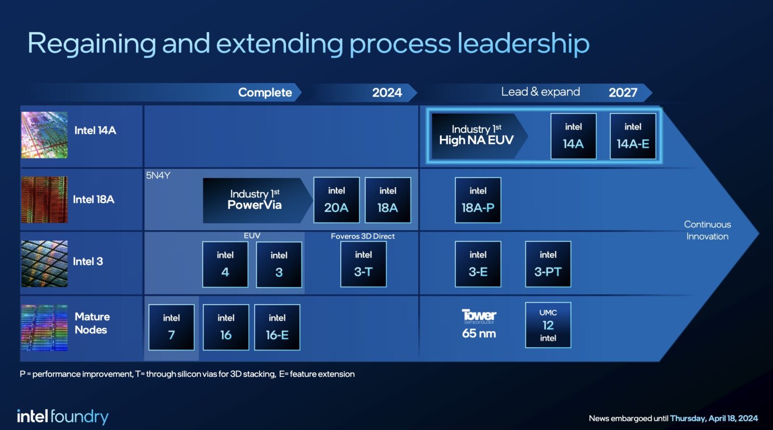
Also, it is my understanding that the primary advantage of High NA (which I believe Intel plans to pilot along side of 18A, but not for production), is that it allows fewer passes since it can cut the same channel without multi-patterning. If that is the case, it seems like Intel would have a chance to leap-frog TSMC sometime in the future by getting to High NA first ...... just as TSMC did with EUV over Intel who held onto DUV way past the point where it was clear that new die shrinks would require EUV.
You don't understand properly. 7nm doesn't NEED EUV. TSMC N7 has no EUV and is just fine. EUV is overly similistic scapegoat for i10nm problems. I have written about the topic at length before but I don't feel like repeating myself. So just dig around if you care. TLDR the probems were poor process deffinition even with the information intel had at the time and poor risk managment. Per Mark Phillips and prior SPIE papers 18A doesn't really have very many multipatterned layers. There is some tip to tip issues, but nothing resoultion related. So even if Intel brought in high-NA for 18A it wouldn't really do very much. Intel also showed off directional etch results which were pretty meh. But as the process matures maybe it makes sense to change the one or two multi pass layers MP mentioned to single pass with CD elongment.
I know this is what Intel said in Q2 2024, but I am guessing this is already slipped by a year:
What piece of information in the past 6mo makes you think 14A has slipped 12mo?
TSMC on the other hand is saying no High NA until 2030!
1. TSMC has never said that.
2. TSMC got their first high-NA tool earlier this year
3. When intel thinks it is ready they will insert it and when TSMC thinks it is ready they will insert it
4. The earliest TSMC can reasonably insert high-NA would be at A14 (as N2/A16 are a pair). I doubt it would ever make sense to rip out existing low-NA tools for layers that might be simplier with high-NA. Since high-NA wasn't avaliable for HVM 2-3 years ago it missed the insertion window for N2/A16.
4. Based on TSMC's statement of development time for new nodes increasing and still sticking to two process development teams, A14 will be launching products in that 2028/29 timeframe.
5. In this day and age TSMC ramps processes to a higher maxium capacity than intel at peak ramp. TSMC needs to secure more tools to adopt high-NA than intel does.
For the above reasons I am not overally concerned for TSMC. Maybe ASML is ready in time for intel to ramp the version of 14A with high-NA and intel gets "the win". If that does occur, yes that would be a nice thing for 14A wafer cost compared to N2/A16, but we aren't talking some coup that will cause N2 to utilization to collapse.