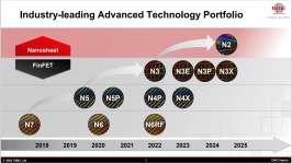
Array
(
    [content] => 
    [params] => Array
        (
            [0] => /forum/threads/tsmc-introduces-latest-n2-and-n3-innovations-at-2023-technology-symposium.18680/
        )

    [addOns] => Array
        (
            [DL6/MLTP] => 13
            [Hampel/TimeZoneDebug] => 1000070
            [SV/ChangePostDate] => 2010200
            [SemiWiki/Newsletter] => 1000010
            [SemiWiki/WPMenu] => 1000010
            [SemiWiki/XPressExtend] => 1000010
            [ThemeHouse/XLink] => 1000970
            [ThemeHouse/XPress] => 1010570
            [XF] => 2021770
            [XFI] => 1050270
        )

    [wordpress] => /var/www/html
)

TSMC Introduces Latest N2 and N3 Innovations at 2023 Technology Symposium

Daniel Nenni

Admin
Staff member
1693491364938.png

TSMC Roadmap 2022

TSMC showcased its industry-leading advanced logic, specialty, and TSMC 3DFabric™ silicon stacking and advanced packaging technologies at its 29th Technology Symposium. Headlining this year’s events were TSMC’s innovative nanosheet-based 2nm technology, its most comprehensive 3nm technology portfolio to meet customers’ diverse product demands, and its industry-first N3AE solution that gives customers a head start on automotive product design to shorten product time-to-market. Hosting in-person and virtual events in parallel this year, TSMC attracted record attendance of more than 8,000 visitors in North America, Taiwan, Europe, China, and Japan, indicating continued strong customer interest in the Company.

Our customers never stop finding new ways to harness the power of silicon to create innovations that shall amaze the world for a better future. In the same spirit, TSMC never stands still, and we keep enhancing and advancing our process technologies with more performance, power efficiency, and functionality so their pipeline for innovation can continue flowing for many years to come.
- Dr. C.C. Wei, CEO of TSMC

Major Technology Highlights at the 2023 Technology Symposium Include​

img_01.png

Customer trust and long-term partnerships are the bedrock to TSMC’s success. This year, TSMC also invited heavyweight customers from around the globe to share collaborative breakthroughs in artificial intelligence (AI), 5G communication, high-performance computing (HPC), and automotive applications. In addition, this year’s Innovation Zone featured 48 emerging startup customers who shared their world-changing innovative technologies and products. These covered high-profile applications such as power-efficient AI chipsets, automotive controllers, gallium nitride (GaN) power modules, energy-harvesting controllers, and medical sensors. The attendee-voted Demo of the Year Award entered its second year this year and had expanded from North America to include Europe. Ambiq was voted the North America award winner for its real-time heart-monitoring solutions driven by edge AI and ultra-low power technologies, while Cambridge GaN Devices was most popular in Europe for its high-performing, energy-saving GaN power modules for consumer electronics, data center power supplies, and electric vehicle (EV) on-board chargers.

Customers Around the Globe Share Their Insights and Successful Stories of Collaborating with TSMC​

img_02.png

Semiconductors have become critical to drive the 21st century economic growth and human progress. HPC, mobile, automotive, and Internet of Things (IoT) applications continue to fuel chip demand and growth, which is a testament to how the world runs on semiconductors. TSMC will continue to invest in its technology advancements, enhance its 3D IC capabilities, and expand its capacity and global manufacturing footprint to meet global customer demands, to help unleash customer innovations, and to achieve a better, safer, and greener future together.
 

Attachments

  • 1693491354071.png
    1693491354071.png
    713.8 KB · Views: 558
That is quite the customer line up. The N3 family is looking dominant! I will be at the OIP conference in Santa Clara. It would be great to meet you!

Happy 15th anniversary OIP!
 
It only just crossed my mind, but I wonder how TSMC arrived at the 1.6x density and 1.18x performance per watt on N3E? Per the finflex paper 2-1 is 1.6 and 1.11, 2-2 is 1.4x and 1.23, and the 2-3 is 1.2x and 1.32. Using their normal ARM 7 core logic density 1.6 would correspond to the 2-1 lib, so that checks out. Some might say they should measure the 2-2 as that is the main HD lib with the 2-1 being reserved for always on applications, but I don't really care as long as they use the wording maximum possible theoretical density and let us know how the different 2-x libs differ (which they did).

Performance on the other hand is a head scratcher. 18% is well above the 2-1 and well bellow the 2-2. If we were going with maximum possible with the HD lib why not give the 32% number? Since the 2-1 was used for density I could also see an argument for saying N3E is 11% improved over N4P. Maybe they were doing an SOC designed in realistic mix of all the 2-x libs to get their 18% performance? But if this was the case why not also use this for the density claim too? Also if they were using all of the libs in some weighted avg, I am surprised the performance isn't higher (but maybe the 2-1 will be more common and the 2-3 less common in real designs than I thought).

Ah, the magic of benchmarketing. Back in the Morris Chang days TSMC was much more conservative about benchmarking numbers but Samsung was not. The result was TSMC having to explain to customers why Samsung was lying. Never a good conversation especially on investor calls. CC Wei is a much more competitive person fighting fire with fire. I'm sure there is a perfectly rational explanation of how they arrived at those numbers but when the chips come out you will see quite a bit of variation.

The customer foundry teams rely on PDKs to determine what the best process is for their specific designs so these benchmarketing numbers are meaningless.
 
Ah, the magic of benchmarketing. Back in the Morris Chang days TSMC was much more conservative about benchmarking numbers but Samsung was not. The result was TSMC having to explain to customers why Samsung was lying. Never a good conversation especially on investor calls. CC Wei is a much more competitive person fighting fire with fire. I'm sure there is a perfectly rational explanation of how they arrived at those numbers but when the chips come out you will see quite a bit of variation.
I have no doubt the numbers are correct with respect to whatever it is they are measuring. Even ignoring the legal requirements to be honest, they are all within the upper and lower bounds of their writings on N3E. I was just curious what methodology was used to arrive at them.
The customer foundry teams rely on PDKs to determine what the best process is for their specific designs so these benchmarketing numbers are meaningless.
That's the funny thing isn't it. If memory serves a while ago CC said something to the tune of "...the people who need to know know..." in reference to data sparseness for N3/E. A fine mantra even if it is irksome to those on the outside. Regardless it is as you say, PDKs and especially testchips matter far more than any white or marketing papers as customers aren't buying powerpoints.
 
I have no doubt the numbers are correct with respect to whatever it is they are measuring. Even ignoring the legal requirements to be honest, they are all within the upper and lower bounds of their writings on N3E. I was just curious what methodology was used to arrive at them.

That's the funny thing isn't it. If memory serves a while ago CC said something to the tune of "...the people who need to know know..." in reference to data sparseness for N3/E. A fine mantra even if it is irksome to those on the outside. Regardless it is as you say, PDKs and especially testchips matter far more than any white or marketing papers as customers aren't buying powerpoints.

Do you think Apple will deliver N2 based SoCs in 2025?
 
It only just crossed my mind, but I wonder how TSMC arrived at the 1.6x density and 1.18x performance per watt on N3E?
From what I have seen at TSMC Tech symposiums and OIP events, TSMC measures performance/density/power of new processes using representative designs taken through P&R, using whatever rev of the PDK and characterized library they have at the time. TSMC will generally spell out what kind of representative design was used during some of their go-deep sessions.
 
Last edited:
It's unlikely to happen. A19 in 2025 would most likely be based on N3P, and A20 in 2026 on N2. It's possible to introduce a M-chip in N2 earlier but will still be in 2026. So, no product will be in the maket in 2025 based on TSMC N2
If that happens then TSMC's 4 year process development/ramp cadence was extended from 4 years to 6 years as N5 was shipping millions of iPhones at the end of 2020.
 
Back
Top