While the foundry (semiconductor contract manufacturing) process is applied to the 'logic die', which serves as the brain of the 6th generation high-bandwidth memory (HBM4), for the first time, it is known that the test yield of the logic die produced by Samsung Electronics' foundry division is stable. Analysts say that Samsung Electronics' HBM4 12-layer development and mass production, which has lagged behind in the HBM technology competition, will gain momentum.
According to industry sources on the 16th, the test production yield of logic dies produced by Samsung Electronics' foundry 4nm (nanometer, 1 billionth of a meter) process has exceeded 40%. Considering that the initial test production yield of Baidu chips, which are being mass-produced with the 4nm process, was in the mid-to-late 10% range, this is encouraging. Jeon Young-hyun, head of Samsung Electronics' DS (semiconductor) division (vice chairman), is known to have delivered a message of encouragement regarding the recent performance of the foundry division.
The foundry division has introduced a large number of new processes that can improve performance while producing this logic die. An official from the semiconductor industry explained, "The initial test production yield of 40% is a good number that is enough to push ahead with the business right away," adding, "Usually, (the foundry process) starts at the 10% level and the yield increases as it goes through mass production."
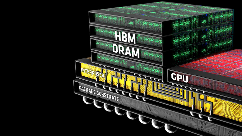
Samsung Electronics, which has surrendered its leadership to SK hynix and Micron in the HBM3E (5th generation HBM) market, is focusing on HBM4 logic die production. HBM4 logic dies are equipped with foundry micro-processing to improve chip performance and can be produced according to the design desired by customers, allowing them to flexibly respond to the 'customized HBM' market, which is rapidly increasing in demand from global Big Tech companies. SK hynix and Micron have to rely on TSMC, a foundry company, but Samsung Electronics can demonstrate its strengths by having its own foundry technology.
Now, the success or failure of Samsung Electronics' HBM4 business depends on the 10nm-class 6th generation (1c) DRAM developed by the Memory Division. The HBM4 12-speed product is equipped with 1c DRAM along with a logic die. Samsung Electronics' competitor SK hynix is using the previous generation DRAM, 1b DRAM, for HBM4, and if Samsung Electronics can mass-produce 1c DRAM stably, it can gain an advantage in HBM4 performance.
Packaging that combines 1c DRAM and logic die to produce them in the form of a final product is also key. Samsung Electronics uses a different packaging method than SK hynix. Samsung Electronics uses 'Advanced Heat-Pressed Non-Conductive Adhesive Film (TC-NCF)' technology, which is a method of laying film-type materials on top of each chip up to a 12-layer HBM product. However, this packaging method is evaluated as having difficulty controlling heat generation.
A semiconductor industry official said, "Samsung Electronics still has the task of stabilizing the DRAM installed in HBM and the technology that packages it."
Meanwhile, SK hynix took the throne of the DRAM market for the first time since its foundation in the first quarter with an HBM market share of more than 70%. According to Counterpoint Research, a market research firm, SK hynix accounted for 36% of the DRAM market share in the first quarter of this year, followed by Samsung Electronics with 34%. SK hynix has produced HBM4 12-layer products and sent samples to customers.

 biz.chosun.com
According to industry sources on the 16th, the test production yield of logic dies produced by Samsung Electronics' foundry 4nm (nanometer, 1 billionth of a meter) process has exceeded 40%. Considering that the initial test production yield of Baidu chips, which are being mass-produced with the 4nm process, was in the mid-to-late 10% range, this is encouraging. Jeon Young-hyun, head of Samsung Electronics' DS (semiconductor) division (vice chairman), is known to have delivered a message of encouragement regarding the recent performance of the foundry division.
The foundry division has introduced a large number of new processes that can improve performance while producing this logic die. An official from the semiconductor industry explained, "The initial test production yield of 40% is a good number that is enough to push ahead with the business right away," adding, "Usually, (the foundry process) starts at the 10% level and the yield increases as it goes through mass production."
Samsung Electronics, which has surrendered its leadership to SK hynix and Micron in the HBM3E (5th generation HBM) market, is focusing on HBM4 logic die production. HBM4 logic dies are equipped with foundry micro-processing to improve chip performance and can be produced according to the design desired by customers, allowing them to flexibly respond to the 'customized HBM' market, which is rapidly increasing in demand from global Big Tech companies. SK hynix and Micron have to rely on TSMC, a foundry company, but Samsung Electronics can demonstrate its strengths by having its own foundry technology.
Now, the success or failure of Samsung Electronics' HBM4 business depends on the 10nm-class 6th generation (1c) DRAM developed by the Memory Division. The HBM4 12-speed product is equipped with 1c DRAM along with a logic die. Samsung Electronics' competitor SK hynix is using the previous generation DRAM, 1b DRAM, for HBM4, and if Samsung Electronics can mass-produce 1c DRAM stably, it can gain an advantage in HBM4 performance.
Packaging that combines 1c DRAM and logic die to produce them in the form of a final product is also key. Samsung Electronics uses a different packaging method than SK hynix. Samsung Electronics uses 'Advanced Heat-Pressed Non-Conductive Adhesive Film (TC-NCF)' technology, which is a method of laying film-type materials on top of each chip up to a 12-layer HBM product. However, this packaging method is evaluated as having difficulty controlling heat generation.
A semiconductor industry official said, "Samsung Electronics still has the task of stabilizing the DRAM installed in HBM and the technology that packages it."
Meanwhile, SK hynix took the throne of the DRAM market for the first time since its foundation in the first quarter with an HBM market share of more than 70%. According to Counterpoint Research, a market research firm, SK hynix accounted for 36% of the DRAM market share in the first quarter of this year, followed by Samsung Electronics with 34%. SK hynix has produced HBM4 12-layer products and sent samples to customers.
[단독] 삼성전자, HBM 두뇌 ‘로직 다이’ 테스트 수율 안정권… HBM4 12단 개발 탄력
단독 삼성전자, HBM 두뇌 로직 다이 테스트 수율 안정권 HBM4 12단 개발 탄력 HBM4 로직 다이 테스트 수율 40% 돌파 전영현 부회장, 파운드리 사업부 임원들 격려 1c D램, HBM 패키징 기술이 관건