Array
(
    [content] => 
    [params] => Array
        (
            [0] => /forum/threads/samsung%E2%80%99s-3nm-yield-reportedly-below-20-struggling-for-mass-production.20504/page-2
        )

    [addOns] => Array
        (
            [DL6/MLTP] => 13
            [Hampel/TimeZoneDebug] => 1000070
            [SV/ChangePostDate] => 2010200
            [SemiWiki/Newsletter] => 1000010
            [SemiWiki/WPMenu] => 1000010
            [SemiWiki/XPressExtend] => 1000010
            [ThemeHouse/XLink] => 1000970
            [ThemeHouse/XPress] => 1010570
            [XF] => 2021770
            [XFI] => 1050270
        )

    [wordpress] => /var/www/html
)

Samsung’s 3nm Yield Reportedly Below 20%, Struggling for Mass Production

TSMC is manufacturing the newest and most advanced smartphone SoCs from MediaTek and Qualcomm that Samsung smartphones use. It means Samsung's revenue and profit are tightly depending on TSMC's yield, cost, quality, and performance. Turn around Samsung smartphone sales affects TSMC's revenue and profit too. It's really a small world.

Samsung smartphone division generated $24 billion sales out of $52.6 billion Samsung's Q1 2024 revenue.

Let's do simple calculation:
Assumption:
1. AP chip costs ~US$100, GM for AP vendors to be 30%, mobile phone unit price to be US$1500
2. tsmc quarterly revenue: US$18.87B in 2024Q1
3. 50% of Samsung smartphone revenue used chips manufactured by tsmc
Then:
1. $24Bx50%=US$12B; 12B/1.5k=8.kk units, 8Mx(US$100*0.7)=US$0.56B
2. tsmc revenue related to Samsung: 0.56/18.87=2.97%. IF Samsung used 100% tsmc chips, it will be ~6%
3. I believe the number above is over-estimated.
Samsung smartphone revenue might affect tsmc revenue and profit, but it seems negligible.

Another way to look at it is using TSMC's revenue and its distribution by platform. My estimate is that around 8.25% ~ 12.75 TSMC smartphone chips revenue is related to Samsung. Or 3.14% ~ 4.85% of TSMC total revenue is related to Samsung Smartphone segment.

I didn't include those smartphone related chips made by TSMC and sold to Samsung neither by Qualcomm nor by MediaTek. Non smartphone chips (like chips for smart TV) are not included either.

1719443169622.png


1719443246271.png


1719443291002.png
 
Last edited:
Let's do simple calculation:
Assumption:
1. AP chip costs ~US$100, GM for AP vendors to be 30%, mobile phone unit price to be US$1500
2. tsmc quarterly revenue: US$18.87B in 2024Q1
3. 50% of Samsung smartphone revenue used chips manufactured by tsmc
Then:
1. $24Bx50%=US$12B; 12B/1.5k=8.kk units, 8Mx(US$100*0.7)=US$0.56B
2. tsmc revenue related to Samsung: 0.56/18.87=2.97%. IF Samsung used 100% tsmc chips, it will be ~6%
3. I believe the number above is over-estimated.
Samsung smartphone revenue might affect tsmc revenue and profit, but it seems negligible.
Another way to look at it is using TSMC's revenue and its distribution by platform. My estimate is that around 8.25% ~ 12.75 TSMC smartphone chips revenue is related to Samsung. Or 3.14% ~ 4.85% of TSMC total revenue is related to Samsung Smartphone segment.
I didn't include those smartphone related chips made by TSMC and sold to Samsung neither by Qualcomm nor by MediaTek. Non smartphone chips (like chips for smart TV) are not included either.

So roughly about 3-5% of tsmc revenue are contributed by Samsung. When HiSilicon/Huawei counted 10% of tsmc revenue and got banned, what happended to tsmc? Nothing. That 10% was absorbed by other customers immediately, and the market share of Huawei was taken by Xiaomi/Vivo... which also use Qualcomm/MediaTek chips.
 
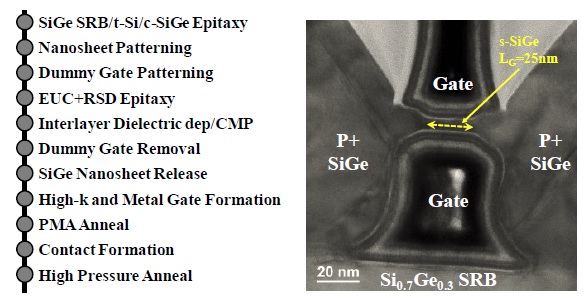
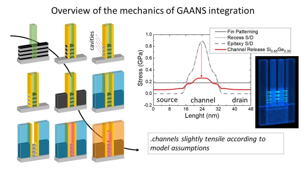
We have heard of many GAA NS benefits: better control of SCE enabling continuous shrinkage of Lg, area efficiency, NS thickness uniformity and width flexibility...but hardly seen practical solutions to two key modules: first one is the PMOS mobility/imbalance and how to solve the stress/mobility loss due to the inner spacers; second one is the so narrow space between nanosheets to fill in high-k metal gate for multiple Vt tuning. Actually, a mid-way device scheme (between FinFET and GAA NS) proposed by Westlake University researchers for Chinese chip industry (in SPIE Advanced Lithography+Patterning conference), the so-called GAA FinFET (I hope they have filed a patent for this), may work for our global semiconductor industry as well:

"For Chinese semiconductor industry, one urgent post-FinFET question is whether we can also evolve into the GAA era with the minimum change of current FinFET process and using the existing (somehow obsolete) manufacturing equipment. The answer is obviously yes and possible tuning/refining schemes to improve the device performance are shown in Fig. 1 (lower part). For example, we can introduce a sacrificial SiGe or oxide layer (like in a SOI wafer) underneath the fin layer and release it for high-K metal gate filling after dummy gate removal. Of course, due to the fin height significantly taller than the (horizontal) NS width, thus formed GAA FinFET may not have a strong electrostatic control of short channels as a GAA NS does."
 

Attachments

  • GAA FinFET.jpg
    GAA FinFET.jpg
    448.4 KB · Views: 177
We have heard of many GAA NS benefits: better control of SCE enabling continuous shrinkage of Lg, area efficiency, NS thickness uniformity and width flexibility...but hardly seen practical solutions to two key modules: first one is the PMOS mobility/imbalance and how to solve the stress/mobility loss due to the inner spacers; second one is the so narrow space between nanosheets to fill in high-k metal gate for multiple Vt tuning. Actually, a mid-way device scheme (between FinFET and GAA NS) proposed by Westlake University researchers for Chinese chip industry (in SPIE Advanced Lithography+Patterning conference), the so-called GAA FinFET (I hope they have filed a patent for this), may work for our global semiconductor industry as well:
Enjoy!
There was also a paper from a Taiwanese uni that I couldn't find with a quick google search about using different Ge conc to enable SiGe PMOS channel.

As for the spacer it is the lesser of two evils. Samsung SF3E didn't have an inner spacer but the consequence is a huge parasitic capacitance hit.

On the topic of NW spacing, I think the bigger problem is not the VTs since dipoles aren't super exotic in this day and age, but rather integration of thick and thin gate devices on the same chip. Separately is easy but on the same die you either have different stack heights and extra processing steps (ie LE for thick gate then cover it to do LE for thin gate), or same stack but no longer having space for gate metal because of the thick Tox. TSMC at their symposium mentioned they weren't going to support native HV devices for N2 and that folks would need to chain together LV devices to do their analog and that they were working on design solutions. What I am curious about is if they will figure out a solution for A14/12, if we see most/all customers move to a new way of doing analog, or if we see disaggregation expand into segments that it hasn't been in before (eg mobile APs/chipsets).
"For Chinese semiconductor industry, one urgent post-FinFET question is whether we can also evolve into the GAA era with the minimum change of current FinFET process and using the existing (somehow obsolete) manufacturing equipment. The answer is obviously yes and possible tuning/refining schemes to improve the device performance are shown in Fig. 1 (lower part). For example, we can introduce a sacrificial SiGe or oxide layer (like in a SOI wafer) underneath the fin layer and release it for high-K metal gate filling after dummy gate removal. Of course, due to the fin height significantly taller than the (horizontal) NS width, thus formed GAA FinFET may not have a strong electrostatic control of short channels as a GAA NS does."
Cool find. I don't really understand how you make anything useful with the last device though.
 
That seems unlikely, given their 3nm is ~not yielding higher than Samsung's, else I suspect Gelsinger would be yodeling such from the mountaintops.

Pat would at least be bragging about having surpassed Samsung's 3nm, without mentioning yields.
I was curious - is there a source on Intel’s 3 process yielding lower than Samsung’s 3nm processes?
 
Enjoy!
There was also a paper from a Taiwanese uni that I couldn't find with a quick google search about using different Ge conc to enable SiGe PMOS channel.

As for the spacer it is the lesser of two evils. Samsung SF3E didn't have an inner spacer but the consequence is a huge parasitic capacitance hit.

On the topic of NW spacing, I think the bigger problem is not the VTs since dipoles aren't super exotic in this day and age, but rather integration of thick and thin gate devices on the same chip. Separately is easy but on the same die you either have different stack heights and extra processing steps (ie LE for thick gate then cover it to do LE for thin gate), or same stack but no longer having space for gate metal because of the thick Tox. TSMC at their symposium mentioned they weren't going to support native HV devices for N2 and that folks would need to chain together LV devices to do their analog and that they were working on design solutions. What I am curious about is if they will figure out a solution for A14/12, if we see most/all customers move to a new way of doing analog, or if we see disaggregation expand into segments that it hasn't been in before (eg mobile APs/chipsets).

Cool find. I don't really understand how you make anything useful with the last device though.
GAA (4-gate) FinFET can be used to replace tri-gate FinFET due to its improved SCE control for continuous scaling while with the minimum change of current mainstream FinFET procee flow (at the lowest cost and possibly with very high yield). The last device scheme in the paper (nanoring-nanowire, or NRW hybrid-channel) is a vertical channel device, which is designed to overcome the shortcoming of vertical nanowire (on-state current too small) by incorporating an extra double-surrounding-gate (DSG) nanoring channel. NRW scheme is very area efficient too.
 
That seems unlikely, given their 3nm is ~not yielding higher than Samsung's, else I suspect Gelsinger would be yodeling such from the mountaintops.
Pat would at least be bragging about having surpassed Samsung's 3nm, without mentioning yields.

Pat only speaks about TSMC, largely ignoring Samsung. Good strategy and it is really upsetting Samsung. Samsung has no big customers so nothing for Intel to poach.

Intel's foundry day was a memorable event while Samsung's foundry event was forgettable. That is a preview of what is to come with Intel 18A and Samsung 2nm, my opinion.
 
I was curious - is there a source on Intel’s 3 process yielding lower than Samsung’s 3nm processes?

That seems unlikely, given their 3nm is ~not yielding higher than Samsung's, else I suspect Gelsinger would be yodeling such from the mountaintops.

Pat would at least be bragging about having surpassed Samsung's 3nm, without mentioning yields.

Source….for a supposition?

Although, I think Pat's character, Intel's decay, and Samsung's missteps, are ripe for statements such as "2nd Place".
 
Pat only speaks about TSMC, largely ignoring Samsung. Good strategy and it is really upsetting Samsung. Samsung has no big customers so nothing for Intel to poach.

Intel's foundry day was a memorable event while Samsung's foundry event was forgettable. That is a preview of what is to come with Intel 18A and Samsung 2nm, my opinion.
I believe there was an interview or two (I think the Ian Cuttress interview recently) where Pat said he thinks with Intel’s own internal business, Intel Foundry is already #2.. I think I’m recalling correctly, but that’s the most I’ve heard Pat talk about Samsung.
 
I believe there was an interview or two (I think the Ian Cuttress interview recently) where Pat said he thinks with Intel’s own internal business, Intel Foundry is already #2.. I think I’m recalling correctly, but that’s the most I’ve heard Pat talk about Samsung.

True, Intel Foundry is #2 today using Samsung math. Samsung includes internal customers, Intel should as well. The difference being that Samsung hides foundry P/L while Intel is being transparent. It is very hard for me to trust a foundry that hides their numbers, right? Even more so when a foundry lies about their numbers! How can a foundry say they are in high volume manufacturing whilst the yield is in single digits?
 
What exactly had happened? 🤔🤔

Typically it is hard to tell. For example, SMIC used to say their 14nm FinFET "SRAM" test chip reached >90% yield but actual product yield at that time was far less than that. CP yield might depend on the process DRM/IP readiness, product spec, design robustness and die size..... D0 is closer to process readiness. It would be better to have Apple-to-Apple comparison, like have Qualcomm Snapdragon products designed and manufactured in different foundries and compared as below. FYI.
1719957664314.png
 
Typically it is hard to tell. For example, SMIC used to say their 14nm FinFET "SRAM" test chip reached >90% yield but actual product yield at that time was far less than that. CP yield might depend on the process DRM/IP readiness, product spec, design robustness and die size..... D0 is closer to process readiness. It would be better to have Apple-to-Apple comparison, like have Qualcomm Snapdragon products designed and manufactured in different foundries and compared as below. FYI.
View attachment 2069

I worked for a commercial SRAM company and we did foundry test chips quite frequently. While SRAM is a good yield point during ramp up, it is not necessarily indicative of final chip yield. And the only time you will see SRAM yield published is when it is good! ;)
 
Back
Top