Of course it's relevant. If you saw first hand how out of the mainstream of the Portland metropolitan area Camas is, you would have the same questions I do. (Gresham would have been a much better choice.) You know a fab isn't like building an auto assembly plant in rural Tennessee, you need a more highly skilled workforce. Why make the hiring process so difficult? It is illogical.Thank you for your explanation, it is your opinion and it is not relevant that I had been in Wafertech or not.
Array
(
    [content] =>
    [params] => Array
        (
            [0] => /forum/threads/q-a-with-tsmc-on-next-gen-foundry.20696/page-2
        )

    [addOns] => Array
        (
            [DL6/MLTP] => 13
            [Hampel/TimeZoneDebug] => 1000070
            [SV/ChangePostDate] => 2010200
            [SemiWiki/EmailDomainReplace] => 1000010
            [SemiWiki/Newsletter] => 1000010
            [SemiWiki/WPMenu] => 1000010
            [SemiWiki/XPressExtend] => 1000010
            [ThemeHouse/XLink] => 1000970
            [ThemeHouse/XPress] => 1010570
            [XF] => 2031070
            [XFI] => 1060170
        )

    [wordpress] => /var/www/html
)
Guests have limited access.
Join our community today!
Join our community today!
You are currently viewing SemiWiki as a guest which gives you limited access to the site. To view blog comments and experience other SemiWiki features you must be a registered member. Registration is fast, simple, and absolutely free so please, join our community today!
You are using an out of date browser. It may not display this or other websites correctly.
You should upgrade or use an alternative browser.
You should upgrade or use an alternative browser.
Q&A With TSMC on Next-Gen Foundry
- Thread starter Daniel Nenni
- Start date
Could you not also argue that intel's fab 4 in Aloha was a middle of nowhere choice back in the 70s? My understanding is that back then it was a swamp and it was also the first fab in the pacific northwest.Of course it's relevant. If you saw first hand how out of the mainstream of the Portland metropolitan area Camas is, you would have the same questions I do. (Gresham would have been a much better choice.) You know a fab isn't like building an auto assembly plant in rural Tennessee, you need a more highly skilled workforce. Why make the hiring process so difficult? It is illogical.
Sooo .. same direct contact BSPD as Intel has demonstrated 2 years ago. Who is doing the "conventional" design?At the same time we have added a very innovative backside power rail design. This backside power rail design allows the customer to move the power supply routing from the front to the back, opening up the space to enhance the performance and at the same time improve the power supply. Our approach is very different from the conventional design for BSPDN - in the conventional backside power rail, you just a drill hole to connect the backside metal to the front side of metal. In doing so you burn space, and you have to enlarge the footprint of the library cell. But in our design, we have very innovative approach - we move the contact or transistor, the source of the transistor to the back without changing the footprint of the library cells. So this clever way allows us to maintain the footprint and provide the maximum flexibility to our customers.
I was in high school and college in the 70s, so I was personally oblivious to the controversy. But I did hear stories about it from people in Oregon when I worked there, that it was very controversial in Intel to diversify away from Silicon Valley. However, Aloha is different than Camas. Aloha was part of the Portland metropolitan area even back then. (So many people were moving to Oregon in the 70s that the governor of Oregon, Tom McCall, was famous for telling people they were welcome to visit Oregon, but implored them not to move there.)Could you not also argue that intel's fab 4 in Aloha was a middle of nowhere choice back in the 70s? My understanding is that back then it was a swamp and it was also the first fab in the pacific northwest.
Sooo .. same direct contact BSPD as Intel has demonstrated 2 years ago. Who is doing the "conventional" design?
While intel did show off BS contacts integrated with their CFET and on a normal GAA device at IEDM 23. I think they gave electrical data comparing the two schemes but you’d have to dig up the paper to confirm that. Intel's powervia doesn't connect to the epi from the backside. Don't know why intel gave us this cartoon and critical pitches but no TEMs at VLSI last year, but here we are. In the linked post I discussed my thoughts on the pros and cons of intel and TSMC's first generation BSPDN implementations. I do hope chip designers don't drag their feet on BSPD beyond A16. Being forced to maintain design rule compatibility with FS N2 and A16 needing to support FSPDN+BSPDN so old N2 IPs can "just work" really gimps TSMC's ability to further shrink cell heights and adds some extra processing cost. Chip designers taking a long time to get comfortable with BSP also hurts intel because they are doing BSPDN only. But I suppose that comes with the territory in logic. It isn't like memory where manufacturing innovation and reducing $/GB is unrestricted by chip designers and their readiness to adopt a new technology.
TSMC Introduces Foundry 2.0
In my understanding, TSMC made the decision not to integrate other foundry chiplets in their packaging due to the current shortage of packaging. It was not a technical decision, purely business which I agree with. Will they open up their packaging to other die in the future? I don't see how they...
semiwiki.com
Last edited:
hist78
Well-known member
All the phases for the TSMC fab in Az are small scale 20K/month compared to the GigaFab of multiphase with >> 100k/month in Taiwan. They are neither cost nor manufacturing efficient for high mix low volume production. The N4 coming online in 2025 and N3/N2 2-4 years later are a good 5 years and a trickle compared to the volume in Taiwan. The need and product mix need is a mess as most demand has moved to the N+1 node and N+2.
Also in small fabs there are always a few steps where one tool is almost capable of supplying all the needs of a phase that make the gigafab for more efficient as well as productive when some thing happens. A small fab like 21 makes expensive choices of 2 tools or maybe 3 for redundancy and run them at very low utilization or just one and when that tool or one of two go down lose 1/2 or 100% of capacity. Makes for operational nightmare for new product and high mix low volume.
The giga fab is the way to go and the small fab in US is all politics not business sense or continuity. If TSMC is serious they need far larger scale.
The real foundry is in Taiwan!
The TSMC Arizona fab phase 1 capacity is intentionally to start smaller than other TSMC Gigafabs. In terms of efficiency and cost it's probably not as good as other Gigafabs too. But it doesn't mean it won't make enough profit to justify the effort. Because the smaller capacity, TSMC can easily push the utilization rate to very high with the support from Qualcomm, Apple, AMD, Nvidia, and Broadcom. For each of these TSMC US customers, to allocate a small percentage of their global orders to TSMC Arizona is easier because this smaller capacity.
This start small strategy will help TSMC, US government, and TSMC's customers to ensure a successful outcome.
Last edited:
Xebec
Well-known member
00:48 - I took Dr. Zhang’s answer on Moore’s Law as a tacit admission that the downward (strong) cost/transistor trend is ending/ended. He talked a lot about high end use of modern nodes, but I didn’t really hear (or forgot?) much about commodity devices other than some enhancements to older nodes.
BruceA
Well-known member
Running a petite fab with none of the burst capacity or flexibility of a giga fab takes huge percentage of limited tool capacity for a high mix low volume. The multiple products likely will run different process versions that require LAH and or warmup and tuneup wafers that in a gigafab you don’t have those contraints. If this doesn’t make sense you have no clue to what is going on in a high mix foundry fab. Cost effective and profitable a big stretch even with subsidies given the schedule and many cost overruns hidden in the schedule slip. Unless their customers accept huge price increase. Why should Apple or anyone else accept a price increase, that is the Foundry’s business problem and they will point to the billions of subsidies that helped them.The TSMC Arizona fab phase 1 capacity is intentionally to start smaller than other TSMC Gigafabs. In terms of efficiency and cost it's probably not as good as other those Gigafabs too. But it doesn't mean it won't make enough profit to justify the effort. Because the smaller capacity, TSMC can easily push the utilization rate to very high with the support from Qualcomm, Apple, AMD, Nvidia, and Broadcom. For each of these TSMC US customers, to allocate a small percentage of their global orders to TSMC Arizona is easier because this smaller capacity.
This start small strategy will help TSMC, US government, and TSMC's customers to ensure a successful outcome.
siliconbruh999
Well-known member
If you are the only foundry for them than it becomes thier problem as wellRunning a petite fab with none of the burst capacity or flexibility of a giga fab takes huge percentage of limited tool capacity for a high mix low volume. The multiple products likely will run different process versions that require LAH and or warmup and tuneup wafers that in a gigafab you don’t have those contraints. If this doesn’t make sense you have no clue to what is going on in a high mix foundry fab. Cost effective and profitable a big stretch even with subsidies given the schedule and many cost overruns hidden in the schedule slip. Unless their customers accept huge price increase. Why should Apple or anyone else accept a price increase, that is the Foundry’s business problem and they will point to the billions of subsidies that helped them.
BruceA
Well-known member
Given TSMC’s financials for Q2 hard to imagine they are hurting. Of course every company from TSMC to its suppliers like ASML or AMAT or their customers like Apple or AMD, Nvidia is in a space all its own, LOLIf you are the only foundry for them than it becomes thier problem as well
Every CEO needs to dance between maximizing value for shareholders and also his customers and suppliers
I guess smartphones will become more of a revenue driver rather than a technology driver. One note is that Kevin Chang mentioned customers can freely choose to have BSPD or not for the A16, with HPC expected to use BSPD and smartphones expected to use it without BSPD.00:48 - I took Dr. Zhang’s answer on Moore’s Law as a tacit admission that the downward (strong) cost/transistor trend is ending/ended. He talked a lot about high end use of modern nodes, but I didn’t really hear (or forgot?) much about commodity devices other than some enhancements to older nodes.
And looking after their staff no?Given TSMC’s financials for Q2 hard to imagine they are hurting. Of course every company from TSMC to its suppliers like ASML or AMAT or their customers like Apple or AMD, Nvidia is in a space all its own, LOL
Every CEO needs to dance between maximizing value for shareholders and also his customers and suppliers
TSMC Washington is a poor example.
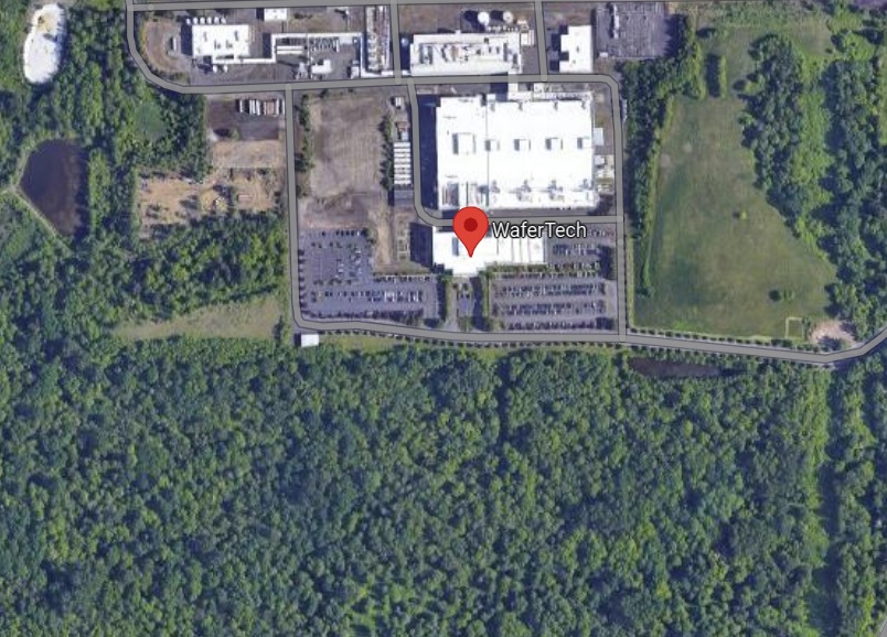
TSMC’s First US Fab - Semiwiki
TSMC originally brought the pure-play foundry business to the United States in 1996 through a joint venture with customers Altera, Analog Devices, ISSI, and private investors (no government money). Altera is now part of Intel but ADI is still a top TSMC customer and enthusiastic supporter. I...
agree with blueone.Yeah, for a long time, for Morris Chang, WaferTech was the "Oregon Fab". Imagine how employees must have felt when the founder doesn't even know where your fab is. I remember when WaferTech was renamed TSMC Washington. I think TSMC made the change just for Morris.
circa 1997 I was looking for a process engineering job with about 10 year experience under my belt. I never heard anything about opportunities at WaferTech. I hired tens of process engineers over the next 10 years. Several who came out of WaferTech. Never lost a process engineer to WaferTech. They seemed invisible. The location they picked seems very odd. The Linear (now ADI) fab up there is also strange, oddly it is 6 inch not 8 inch.