Where did you get this information? To my knowledge, all MJ said during the earnings call was to dual-source for Nova Lake.Sorry, but that's simple not true. If it was capacity then they wouldn't be doing their high end SKU on N2. High end SKUs are lower volume than the mid range SKUs and they need the extra performance from the N2 node.
Array
(
    [content] =>
    [params] => Array
        (
            [0] => /forum/threads/potential-ceo-candidate-for-intel.22039/page-3
        )

    [addOns] => Array
        (
            [DL6/MLTP] => 13
            [Hampel/TimeZoneDebug] => 1000070
            [SV/ChangePostDate] => 2010200
            [SemiWiki/EmailDomainReplace] => 1000010
            [SemiWiki/Newsletter] => 1000010
            [SemiWiki/WPMenu] => 1000010
            [SemiWiki/XPressExtend] => 1000010
            [ThemeHouse/XLink] => 1000970
            [ThemeHouse/XPress] => 1010570
            [XF] => 2031070
            [XFI] => 1060170
        )

    [wordpress] => /var/www/html
)
Guests have limited access.
Join our community today!
Join our community today!
You are currently viewing SemiWiki as a guest which gives you limited access to the site. To view blog comments and experience other SemiWiki features you must be a registered member. Registration is fast, simple, and absolutely free so please, join our community today!
You are using an out of date browser. It may not display this or other websites correctly.
You should upgrade or use an alternative browser.
You should upgrade or use an alternative browser.
Potential CEO Candidate for Intel
- Thread starter Artificer60
- Start date
It's a rumour. From Exist50 from reddit. Also Intel themselves said that some CPU dies would have external sourceWhere did you get this information? To my knowledge, all MJ said during the earnings call was to dual-source for Nova Lake.
"And as I said, we're very happy with where we are from a performance and yield perspective at this point in the process. So, that will stay on 18A. Then as you look forward, to our next-generation product for client after that, Nova Lake will actually have die both inside and outside for that process. So, you'll actually see compute tiles inside and outside."It's a rumour. From Exist50 from reddit. Also Intel themselves said that some CPU dies would have external source
They didn't mention CPU dies. Since Nova Lake is a desktop product line, one of the design criteria should be cost. If they can use an older processes from TSMC for some of the dies in the package to lower cost, they should.
Intel (INTC) Q4 2024 Earnings Call Transcript | The Motley Fool
INTC earnings call for the period ending December 31, 2024.
compute tiles means CPU tiles"And as I said, we're very happy with where we are from a performance and yield perspective at this point in the process. So, that will stay on 18A. Then as you look forward, to our next-generation product for client after that, Nova Lake will actually have die both inside and outside for that process. So, you'll actually see compute tiles inside and outside."
They didn't mention CPU dies. Since Nova Lake is a desktop product line, one of the design criteria should be cost. If they can use an older processes from TSMC for some of the dies in the package to lower cost, they should.

Intel (INTC) Q4 2024 Earnings Call Transcript | The Motley Fool
INTC earnings call for the period ending December 31, 2024.www.fool.com
I don't think they explicitly stated that based on the transcript. It could be just like the Meteor Lake arrangement.compute tiles means CPU tiles
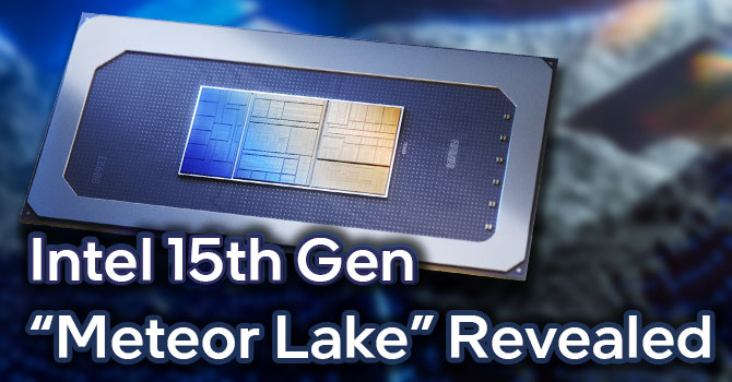
In both Meteor Lake, Lunar lake and Arrow lake, the tile that contains the CPU cores is called the compute tile. Practically, every online publication refers to it like this:I don't think they explicitly stated that based on the transcript. It could be just like the Meteor Lake arrangement.
Intel Meteor Lake Technical Deep Dive
Today Intel is taking the wraps off their Meteor Lake Architecture. Our tech preview tells you everything you need to know about Intel's new ideas that will power the company's processors for years to come. Just like AMD, Intel is betting on chiplets, which combine multiple silicon dies into a...
www.techpowerup.com
The Compute tile is where the all important CPU cores are located.
If we assume this rumor is true, when one looks at things by the numbers, so what? The U/P/H laptop segments are 80% of intel's volume. If 95+% of the laptop parts that make up 80% of Intel's sales AND the majority of the remaining 20% desktop parts don't use TSMC, then intel is seemingly continuing to in-source more of their production rather than re-outsourcing. That is just the CPU too, what about the SOC dies, IO dies, and chipsets. I don't recall seeing any rumors of Intel continuing to outsource those, and Intel 3-E implies a desire to move those higher volume dies back internal. Intel saying that Intel 4/3 capacity starts strongly increasing in 2026-2028 also supports comments of a move from 30-40% outsourcing towards 10% outsourced Si by the end of the decade. Although how much Intel products overforcasting their product demands impacts things is hard to say. Although I suspect the main impact would be with total units rather than the exact composition of what said units are made of.The fact that they are using TSMC N2 for Nova Lake high end NVL-SK / NVL-HX is
1) Intel's goal was unquestioned process performance per watt leadership in 2025. N2 doesn't launch in anything until 2026. If 18A does indeed land between N3 and N2 not only does Intel meet their public objective, that isn't even a particularly bad place to be given how small the difference between N3 and N2 is (assuming TSMC hits their targets as they usually have recently).an indication that Intel 18A has inferior performance. They have to use N2 if they want to compete with AMD.
2) Intel has shown time over time that they will happily pay premiums fabless companies wouldn't pay for even for the most modest of performance improvements. I don't know if it really matters so much being able to see "we are the fastest". If N2 allowed for a chip even 1% faster, I wouldn't be shocked if CCG said "SOLD". An example is copper RDL layers. TSMC is only now rolling out Cu for these layers after decades of using Cu for the rest of the metal layers because for whatever reason TSMC and or their customers thought the trivial cost adder wasn't worth the performance adder. Intel on the other hand has been using Cu for RDL basically since they started using Cu at 130nm. With that knowledge, I don't know if the information that Intel is using N2 for premium flagship SKUs that are really there to market the rest of the SKU stack is enough to condemn 18A as being unable to create chips comepetive with N3 AMD stuff (since they are slower to move to new nodes). After all, we aren't talking about 14nm+++ vs N7P or intel 7 vs N5P. Even TSMC thinks the gap is at worst single digit percent when one compares their statements to TSMC's self-reported PPA claims.
3) Something various back and forths with IanD made me wonder was maybe Intel's BSPDN implementation has no issue with laptop/server or "sane" HPC designs from foundry customers. But it is undeniable that Intel's i9-K desktop chips are in a league all of their own for thermal density. Practically the only stuff that runs "hotter" are power electronics. Maybe BSPDN design/cooling need to become more advanced and or per FET power consumption need to go down further before you can start seeing those 6 GHz overclockable high core count CPUs being practical. Then for those lower thermal density parts like laptop CPUs, server CPUs, or GPUs can run just fine as Intel demonstrated with their blue sky creek test chip.
Also, I don't know if using N2 at all is a complete admission of 18A failure. For one, if rumors are to be believed and Intel is using N2 for large core count CPU "tiles", then a choice to use N2 would have needed to have been finalized in 2022 at the absolute latest. Given Intel products' insistence on using custom IPs and interfaces rather than standard licensable versions, design work on all the IPs Intel would need to even begin designing an N2 CPU die would have likely started in that 2020 or 2021 timeframe. Back in 2020 Intel was planning on a fab-lite strategy, and in 2022 18A would have been more uncertain than it is now and without the final successes of Intel 4 and 3 to build credibility.
If I put myself in the shoes of a CCG VP and I started work on an N2 design back in the Bob Swan days, then Pat came in and said you will need to start work on 18A, of course I would still want to continue N2 work in parallel in case things blew up. If I go ahead with that, in 2022/2023 I have all or most of my IPs ready to go. At that time if I need to switch most or all of my volume to N2 I can rush through a wafer agreement or amendment to an existing one with TSMC so they will be able to build out the capacity required to support my demands. Since 18A hasn't seemed to blow up, I wouldn't need the nuclear option. But it seems like a waste designing an N2 Nova lake to never make any money on it. Might as well do the last little bit of work to finish her up and launch a low volume SKU so I can at least get some return on that investment. I also get to use my N2 design as a bargaining chip to get better 18A pricing from Intel foundry. If it performs that little bit better than 18A all the better for my product's competitiveness, especially since AMD will be sitting in their corner on some N3P or N3X thing. Seems like a win-win for my department without kneecapping Ann/Kievan/Naga's new business like outsourcing mobile or SOC had done.
As long as 18A products show a large reduction in foundry losses and ideally also an improvement to intel products closer towards what a normal fabless peer of intel can demonstrate (from an operating margins perspective) then I don't exactly think the "house is lost" even if 18A was somehow worse than N3P for HPC products. Betting the house refers to putting all of your money into a venture or bet. If That money generates a positive return you can't by definition have "lost the house".Remember they said "Intel is betting the house on 18A"? Well, it looks like they lost the house!
TSMC spent most of its existence without the fastest node, and they had no problem growing. It is about service. Best node helps a ton, but isn't a requirement for foundry success. IMO being competitive should be more than sufficient to "get people into the door" as it were. The rest comes to foundry fundamentals and incremental building trust design win by design win contract by contract.It does matter. If you don't have the fastest node it's going to get hard to get foundry customers.
See my earlier comment. If intel is only outsourcing the large die desktop versions of the CPU tile that means over 85% of CPU tiles are not outsourced. Certainly better than 0% internal we see now. Intel foundry would gladly trade TSMC 100% of desktop CPU dies if Intel could get the chipsets, PCH, and PCD dies back from TSMC but mostly Samsung. They would laugh all the way to the bank while intel and AMD fans argue until the cows come home over the desktop i9s that are at the end of the day irrelevant to Intel's finical performance.And if your own multi-billion fabs are under utilised because you have to use competitors node you are going to lose money.
I don't agree with your sentiment. I just don't see any indication this is happening. By sending various parts of the die to less advanced processes, the complete collapse of DCAI unit shipments (massive TAM shrinkage combined with MSS losses declining revenue and claimed ASP increases), and CCG shipments (TAM at/below pre-pandemic levels for the near term and losing market share to Qualcomm with modest share loss to AMD) intel should have wafer requirements lower than they've had in a VERY LONG time. I don't see any indication to think that desktop Nova lake CPU "tiles" would be the straw that would break the Carmel's back and cause capacity issues. After all, Intel literally did publicly push out the German fabs, Ohio fabs, Malaysia advanced packaging fab, and position Ohio as more of 14A site than an 18A site as of late. One doesn't do that if you are capacity constrained.They are using TSMC cause they don't have that much capacity on 18A we will have Panther Lake ,Nova Lake,Clearwater Forest Diamond Rappids and wildcat lake plus external tape out in H1 25 so EOY 26 Production?
I think we need to wait for more information. Die can mean graphic tile, SoC tile, etc. They did not explicitly say CPU die during the earning call.In both Meteor Lake, Lunar lake and Arrow lake, the tile that contains the CPU cores is called the compute tile. Practically, every online publication refers to it like this:
Intel Meteor Lake Technical Deep Dive
Today Intel is taking the wraps off their Meteor Lake Architecture. Our tech preview tells you everything you need to know about Intel's new ideas that will power the company's processors for years to come. Just like AMD, Intel is betting on chiplets, which combine multiple silicon dies into a...www.techpowerup.com
Meteor Lake - Wikipedia
It's pretty clear that compute tile means the tile the CPU resides in, but it you want to believe otherwise I will not stop youI think we need to wait for more information. Die can mean graphic tile, SoC tile, etc. They did not explicitly say CPU die during the earning call.
Meteor Lake - Wikipedia
en.wikipedia.org
You are right. I searched with key word "compute tile":It's pretty clear that compute tile means the tile the CPU resides in, but it you want to believe otherwise I will not stop you
"And as I said, we're very happy with where we are from a performance and yield perspective at this point in the process. So, that will stay on 18A. Then as you look forward, to our next-generation product for client after that, Nova Lake will actually have die both inside and outside for that process. So, you'll actually see compute tiles inside and outside."
MKWVentures
Moderator
Intel decisions at this point are not technical... They are financial. And they have serious issues on financing due to foundry group spending and losses. Intel could have the best 2nm GAA technology in the world and it doesnt matter. Its still could be too expensive and require too much cash to try to ramp the fabs unless they are full with committed products.... which they are not.Sorry to say this, but I think Intel are boned. The fact that they are using TSMC N2 for Nova Lake high end NVL-SK / NVL-HX is an indication that Intel 18A has inferior performance. They have to use N2 if they want to compete with AMD.
Remember they said "Intel is betting the house on 18A"? Well, it looks like they lost the house!
MKWVentures
Moderator
Please ask Intel what the margins are expected to be on 18A in 2026.But regardless, from a margin optimization perspective, they need to drive as much volume as possible to their foundry to achieve break-even for IF by 2027.
I have low expectations. Just break even with IF first, as that would at least prevent Intel's overall valuation from being dragged down, as what is currently being painted by the sell side.Please ask Intel what the margins are expected to be on 18A in 2026.
They have mentioned multiple times that increased EUV utilization will improve margins.
MKWVentures
Moderator
Yes, they said that..... Im just talking 18A. will the OM be positive or negative in 2026They have mentioned multiple times that increased EUV utilization will improve margins.
Doesn't really matter negative in 2026 or not. Just make sure the trend moving in the direction to break even by 2027. I really don't care how they do it. Just do that first.Yes, they said that..... Im just talking 18A. will the OM be positive or negative in 2026
When does Intel's first high NA EUV node, Intel 14A come online? In what lake will it first swim? Several news reports from months ago suggest some Nova Lake skus will be on 14A. All MJ said is that Nova Lake will have compute die from inside and outside. Maybe some Nova Lake will be on 14A and those will be the highest end skus.... who knows? There is also an improved variant of 18A, called 18A-P, and there are improved variants of TSMC N2 as well, N2P and N2X. At this point we don't know how all these nodes will compare. But the bottom line is Intel is back in the game, period. Intel Foundry represents the first threat TSMC has ever had to its ~ 7 year process leadership.You are right. I searched with key word "compute tile":
"And as I said, we're very happy with where we are from a performance and yield perspective at this point in the process. So, that will stay on 18A. Then as you look forward, to our next-generation product for client after that, Nova Lake will actually have die both inside and outside for that process. So, you'll actually see compute tiles inside and outside."
When does Intel's first high NA EUV node, Intel 14A come online? In what lake will it first swim? Several news reports from months ago suggest some Nova Lake skus will be on 14A. All MJ said is that Nova Lake will have compute die from inside and outside. Maybe some Nova Lake will be on 14A and those will be the highest end skus.... who knows? There is also an improved variant of 18A, called 18A-P, and there are improved variants of TSMC N2 as well, N2P and N2X. At this point we don't know how all these nodes will compare. But the bottom line is Intel is back in the game, period. Intel Foundry represents the first threat TSMC has ever had to its ~ 7 year process leadership.
But seriously, has Intel updated HNA-EUV plans since Pat left?
Remember, it all comes down to the PDK. Will HNA-EUV be easier to design to? Will it be more cost effective? How will it compare to the non HNA-EUV node from TSMC in regards to PPA? There has to be a good ROI for customers to take the risk of being first.
The Intel and TSMC foundry events are coming up in April. If TSMC does not mention HNA-EUV that means customers are not pressuring them for it. It really is all about the top 10 customers and what they want.
Just my opinion of course.
I doubt that High NA will be featured in TSMC's A14, at least not in the first generation. Currently, top customers are primarily focusing on advanced packaging and HBM to enhance performance, making the High NA option relatively expensive and risky. Apple seems to be shifting its selling points to other areas, possibly AI. Qualcomm and Mediatek are aligned with Apple, while Nvidia and AMD require CoWoS. It would be quite amusing if Intel pressured TSMC to adopt High NABut seriously, has Intel updated HNA-EUV plans since Pat left?
Remember, it all comes down to the PDK. Will HNA-EUV be easier to design to? Will it be more cost effective? How will it compare to the non HNA-EUV node from TSMC in regards to PPA? There has to be a good ROI for customers to take the risk of being first.
The Intel and TSMC foundry events are coming up in April. If TSMC does not mention HNA-EUV that means customers are not pressuring them for it. It really is all about the top 10 customers and what they want.
Just my opinion of course.
