Pat Gelsinger, former CEO of Intel, recently posted on LinkedIn that he joined xLight as executive chairman, and the xLight official website also announced the news in March.
xLight is the company that develops a linear electron accelerator for extreme ultraviolet (EUV) lithography machines, and claims to reduce system and cost by three times, achieve commercialization goals by 2028, and maintain compatibility with existing equipment.
According to Pat Gelsinger, we are entering the most transformative moment of computing infrastructure since the dawn of the Internet. I look forward to working with xLight to further advance the next generation of semiconductor manufacturing." Free electron lasers are the future of exposure technology, and xLight is the clear leader in particle accelerator technology.
Nicholas Kelez, CEO of xLight, said, "Pat Gelsinger, like us, believes that EUV lithography is the key to unlocking the next generation of computing. And when he learns about the work xLight is doing to build the world's most powerful lasers and revolutionize EUV exposure technology, it's the perfect combination. In particular, Pat Gelsinger's technical understanding and knowledge of the semiconductor industry has been outstanding, and he immediately understood how important xLight's system is to the future of semiconductor manufacturing in the U.S., and we are delighted to have him join the Board and look forward to working together."
At present, the EUV lithography machine of ASML, a manufacturer of exposure machines, uses an EUV light source system called laser plasma EUV light source (LPP), which uses a 30kW carbon dioxide laser emitter to irradiate tin metal droplets ejected from the nozzle at a rate of 50,000 drops per second, irradiating them twice per drop (i.e., 100,000 laser photoelements per second), evaporating them into plasma, and then through the transition between the energy levels of high-valent tin ions EUV light at a wavelength of 13.5nm.
However, it is precisely because the EUV-LPP system needs to rely on a powerful high-energy laser beam to evaporate tiny metal droplets, which makes the entire light source system not only huge, but also complex, and also consumes a lot of power, and the power of the EUV light source generated is also limited. At present, only a few of the world's leading wafer manufacturers can afford this EUV lithography machine, which costs about $150 million per unit, for the manufacture of chips made of advanced chips below 7 nanometers.
In recent years, research institutes around the world have been developing new EUV light source systems, so as to bypass the EUV-LPP technology route adopted by ASML and greatly reduce the cost of EUV light source systems. Among them, the EUV light source scheme using free electron laser (FEL) technology is highly promising.
Currently, EUV-FEL technologies are broadly divided into two types, including vibrator FEL and self-amplifying spontaneous emission (SASE) FEL. In an oscillator FIL, an electron beam from an electron accelerator emits light in an oscillator, interacts with the oscillator light stored in the oscillator, and amplifies the FEL light. However, due to the poor reflectivity of mirrors to short-wavelength light, FEL wavelengths are limited to more than 100 nm. Whereas, in the self-amplifying spontaneous emission (SASE) FE, the accelerator provides the spontaneous emission of a high-quality electron beam, which is self-amplifying in a long oscillator without any oscillator and external assistance. It is suitable for short-wavelength FEL, making EUV-FEL technology the main direction of current research.
According to a research paper based on the EUV-FEL light source published by researchers from the High Energy Accelerator Research Organization (KEK) in Tsukuba, Japan, the construction and operating costs of the EUV-FEL light source are roughly estimated to be $400 million for 10kW EUV power and $40 million per year in operating costs. As a result, the construction cost of a 1kW EUV power is approximately US$40 million and the annual transportation cost is US$4 million, compared to a rough estimate of US$20 million and US$15 million per year for 250 W EUV power, which is equivalent to a construction cost of US$80 million per 1 kW EUV power and an operating cost of US$60 million per year, compared to a rough estimate of the construction and operating costs of 250 WEUV and US$15 million per year. Obviously, the construction cost of EUV-LPP light source is twice that of EUV-FEL light source, and the operating cost is 15 times that of EUV-FEL light source.
Overall, the cost of the current EUV-LPP light source is also 3 times that of the EUV-FEL light source. Among them, the maintenance cost of the light collector accounts for the majority of the operating costs, because the light collector lens will deteriorate due to the contamination of tin chips and need to be replaced frequently. In addition, the huge energy consumption is also a major cost. In other words, the use of EUV-FEL light source instead of EUV-LPP light source can reduce the comprehensive cost by more than 2 times.
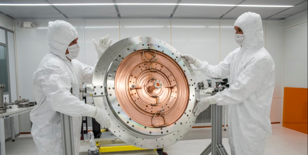
Pat Gelsinger's xLight is developing an EUV lighting system based on ERL's EUV-FEL technology. According to the official website, xLight is led by a team of light source pioneers, exposure engineers, and particle accelerator manufacturers. Although small, the team has many years of experience in the field of exposure and accelerator technology. Among them, in addition to veteran researchers from Stanford linear accelerators and other particle accelerators, its chief scientist, Dr. Gennady Stupakov, is one of two recipients of the 2024 IEEE Society for Nuclear and Plasma Science Particle Accelerator Science and Technology Award (PAST Award).
According to a Linkedin article by Pat Gelsinger, who has just become the executive director of xLight, the EUV-LPP light source system developed by xLight is also four times the power of today's most advanced EUV light source system, that is, about 1000W, and is expected to be ready for commercial application in 2028. XLightg also noted that EUV-LPP is currently the only way to produce EUV light sources for advanced semiconductor manufacturing. However, it is very power-hungry and cannot fully support future versions of the ASML lithography machine, as these versions require a power supply of up to 2 kW.
Pat Gelsinger said that the xLight technology can deliver 4 times the power of current EUV light sources, which can reduce the exposure cost per wafer by about 50 percent, and that a single xLight's EUV-FEL light source system can support up to 20 ASML EUV lithography machines, and the life of the light source system is 30 years, which can reduce capital and operating expenses by more than 3 times, which will be a significant step forward in manufacturing efficiency.
It is important to note that the goal of xLight is not to replace ASML's EUV lithography machine, but to launch an EUV-LPP light source system that can be compatible with ASML's EUV lithography machine, and achieve the goal of using ASML's lithography machine and manufacturing advanced processes by 2028. However, it is unclear whether xLight's EUV-LPP illumination system will be compatible with ASML's High-NA EUV lithography system. However, based on the available information, ASML's High-NA EUV exposure machine is still a technical path using EUV-LPP, so it is expected that a compatible situation will be achieved in the future.
Although EUV-FEL light sources have many advantages over EUV-LPP light sources, they also face the problem of being bulky and difficult to integrate into existing wafer fabrication clean rooms. For example, in the existing standard EUV light source, the light source is located below the machine itself, while in the case of a High-NA EUV lithography machine, the EUV-LPP light source is located on the same horizontal plane, so any other light source system must take these practices into account. If EUV-FEL light sources prove to be commercially valuable, it may be necessary for EUV-FEL light sources to be integrated into the design of next-generation fabs.
It is worth noting that ASML considered switching to EUV-FEL light sources ten years ago, and in recent years has been considering the switch to EUV-FEL light sources again in comparison of the technological advancements of EUV-FEL light sources with the EUV-LPP light source technology roadmap. But in the end, ASML executives decided that the EUV-LPP light source posed less risky and temporarily abandoned the plan to adopt the EUV-FEL light source.
 technews.tw
xLight is the company that develops a linear electron accelerator for extreme ultraviolet (EUV) lithography machines, and claims to reduce system and cost by three times, achieve commercialization goals by 2028, and maintain compatibility with existing equipment.
According to Pat Gelsinger, we are entering the most transformative moment of computing infrastructure since the dawn of the Internet. I look forward to working with xLight to further advance the next generation of semiconductor manufacturing." Free electron lasers are the future of exposure technology, and xLight is the clear leader in particle accelerator technology.
Nicholas Kelez, CEO of xLight, said, "Pat Gelsinger, like us, believes that EUV lithography is the key to unlocking the next generation of computing. And when he learns about the work xLight is doing to build the world's most powerful lasers and revolutionize EUV exposure technology, it's the perfect combination. In particular, Pat Gelsinger's technical understanding and knowledge of the semiconductor industry has been outstanding, and he immediately understood how important xLight's system is to the future of semiconductor manufacturing in the U.S., and we are delighted to have him join the Board and look forward to working together."
At present, the EUV lithography machine of ASML, a manufacturer of exposure machines, uses an EUV light source system called laser plasma EUV light source (LPP), which uses a 30kW carbon dioxide laser emitter to irradiate tin metal droplets ejected from the nozzle at a rate of 50,000 drops per second, irradiating them twice per drop (i.e., 100,000 laser photoelements per second), evaporating them into plasma, and then through the transition between the energy levels of high-valent tin ions EUV light at a wavelength of 13.5nm.
However, it is precisely because the EUV-LPP system needs to rely on a powerful high-energy laser beam to evaporate tiny metal droplets, which makes the entire light source system not only huge, but also complex, and also consumes a lot of power, and the power of the EUV light source generated is also limited. At present, only a few of the world's leading wafer manufacturers can afford this EUV lithography machine, which costs about $150 million per unit, for the manufacture of chips made of advanced chips below 7 nanometers.
In recent years, research institutes around the world have been developing new EUV light source systems, so as to bypass the EUV-LPP technology route adopted by ASML and greatly reduce the cost of EUV light source systems. Among them, the EUV light source scheme using free electron laser (FEL) technology is highly promising.
Currently, EUV-FEL technologies are broadly divided into two types, including vibrator FEL and self-amplifying spontaneous emission (SASE) FEL. In an oscillator FIL, an electron beam from an electron accelerator emits light in an oscillator, interacts with the oscillator light stored in the oscillator, and amplifies the FEL light. However, due to the poor reflectivity of mirrors to short-wavelength light, FEL wavelengths are limited to more than 100 nm. Whereas, in the self-amplifying spontaneous emission (SASE) FE, the accelerator provides the spontaneous emission of a high-quality electron beam, which is self-amplifying in a long oscillator without any oscillator and external assistance. It is suitable for short-wavelength FEL, making EUV-FEL technology the main direction of current research.
According to a research paper based on the EUV-FEL light source published by researchers from the High Energy Accelerator Research Organization (KEK) in Tsukuba, Japan, the construction and operating costs of the EUV-FEL light source are roughly estimated to be $400 million for 10kW EUV power and $40 million per year in operating costs. As a result, the construction cost of a 1kW EUV power is approximately US$40 million and the annual transportation cost is US$4 million, compared to a rough estimate of US$20 million and US$15 million per year for 250 W EUV power, which is equivalent to a construction cost of US$80 million per 1 kW EUV power and an operating cost of US$60 million per year, compared to a rough estimate of the construction and operating costs of 250 WEUV and US$15 million per year. Obviously, the construction cost of EUV-LPP light source is twice that of EUV-FEL light source, and the operating cost is 15 times that of EUV-FEL light source.
Overall, the cost of the current EUV-LPP light source is also 3 times that of the EUV-FEL light source. Among them, the maintenance cost of the light collector accounts for the majority of the operating costs, because the light collector lens will deteriorate due to the contamination of tin chips and need to be replaced frequently. In addition, the huge energy consumption is also a major cost. In other words, the use of EUV-FEL light source instead of EUV-LPP light source can reduce the comprehensive cost by more than 2 times.
Pat Gelsinger's xLight is developing an EUV lighting system based on ERL's EUV-FEL technology. According to the official website, xLight is led by a team of light source pioneers, exposure engineers, and particle accelerator manufacturers. Although small, the team has many years of experience in the field of exposure and accelerator technology. Among them, in addition to veteran researchers from Stanford linear accelerators and other particle accelerators, its chief scientist, Dr. Gennady Stupakov, is one of two recipients of the 2024 IEEE Society for Nuclear and Plasma Science Particle Accelerator Science and Technology Award (PAST Award).
According to a Linkedin article by Pat Gelsinger, who has just become the executive director of xLight, the EUV-LPP light source system developed by xLight is also four times the power of today's most advanced EUV light source system, that is, about 1000W, and is expected to be ready for commercial application in 2028. XLightg also noted that EUV-LPP is currently the only way to produce EUV light sources for advanced semiconductor manufacturing. However, it is very power-hungry and cannot fully support future versions of the ASML lithography machine, as these versions require a power supply of up to 2 kW.
Pat Gelsinger said that the xLight technology can deliver 4 times the power of current EUV light sources, which can reduce the exposure cost per wafer by about 50 percent, and that a single xLight's EUV-FEL light source system can support up to 20 ASML EUV lithography machines, and the life of the light source system is 30 years, which can reduce capital and operating expenses by more than 3 times, which will be a significant step forward in manufacturing efficiency.
It is important to note that the goal of xLight is not to replace ASML's EUV lithography machine, but to launch an EUV-LPP light source system that can be compatible with ASML's EUV lithography machine, and achieve the goal of using ASML's lithography machine and manufacturing advanced processes by 2028. However, it is unclear whether xLight's EUV-LPP illumination system will be compatible with ASML's High-NA EUV lithography system. However, based on the available information, ASML's High-NA EUV exposure machine is still a technical path using EUV-LPP, so it is expected that a compatible situation will be achieved in the future.
Although EUV-FEL light sources have many advantages over EUV-LPP light sources, they also face the problem of being bulky and difficult to integrate into existing wafer fabrication clean rooms. For example, in the existing standard EUV light source, the light source is located below the machine itself, while in the case of a High-NA EUV lithography machine, the EUV-LPP light source is located on the same horizontal plane, so any other light source system must take these practices into account. If EUV-FEL light sources prove to be commercially valuable, it may be necessary for EUV-FEL light sources to be integrated into the design of next-generation fabs.
It is worth noting that ASML considered switching to EUV-FEL light sources ten years ago, and in recent years has been considering the switch to EUV-FEL light sources again in comparison of the technological advancements of EUV-FEL light sources with the EUV-LPP light source technology roadmap. But in the end, ASML executives decided that the EUV-LPP light source posed less risky and temporarily abandoned the plan to adopt the EUV-FEL light source.
Pat Gelsinger 又有新工作,加入 EUV 光源 xLight 任執行董事長
英特爾前執行長 Pat Gelsinger 近日在 LinkedIn 發文,加入 xLight 公司任執行董事長,xLight 官網 3 月也公布消息。 xLight 是開發極紫外光(EUV)曝光機直線電子加速器的自由電子雷射(FEL)光源系統公司,號稱可將系統及成本降低三倍,2028 年達成商業化...
technews.tw