You are currently viewing SemiWiki as a guest which gives you limited access to the site. To view blog comments and experience other SemiWiki features you must be a registered member. Registration is fast, simple, and absolutely free so please, join our community today!
But the decap shows that Panther Lake use HP cell for overall device, no HD cell. And I remember Panther Lake performance is not high ( its clock rate even lower than Arrow Lake), and it emphasizes more on efficiency. So question is why Panther Laker don not just use HD cell?
there could be any number of reasons.
they need the performance
The HP cell has better stability, lower error rate
The layout did not show a penalty for a larger cell. using a HD cell to save 1mm2 might not be a good idea. with chiplets and dummy silicon you could end up with no penalty.
I mentioned to someone on here that 20 years ago, we never used the most dense SRAM. Designers were not going to risk a product to save 2mm2.
The reason for using HD cells is to increase density, and to reduce energy consumption per operation (gate transition) for cases where this matters more than maximum clock speed. For most CPUs HP cells are more appropriate, they're a better fit to the device priorities. For most ASICs HD cells are a better fit to the device priorities. Neither is "better" than the other, they have different pros and cons.
(but stability and error rate are nothing to do with it, at least not in any application I'm aware of...)
Wow, this really surprise me. I originally think ASIC chip may focus on performance over power consumption due to the less limitation on cooling capabilities?
Wow, this really surprise me. I originally think ASIC chip may focus on performance over power consumption due to the less limitation on cooling capabilities?
Some ASICs like NPU/GPU, sure. But most ASICs don't have liquid-cooling systems, and requiring the cooling system to keep the heatsink perhaps 20C cooler -- if there is a heatsink at all! -- is somewhere between difficult/expensive and impossible.
So HPC chips (including CPU/NPU/GPU) tend to use HP libraries and maybe BSPD (but not always, especially if power efficiency is the #1 priority) and other ASICs tend to use HD libraries and FSPD to reduce cost and power consumption (but not always, especially if performance is the #1 priority).
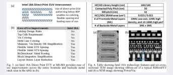
for Intel 18A, Intel R&D was/is confident about 32nm with EUV Low NA 0.33 Direct Print, but can Intel Volume Manufacturing yield?
for Intel 14A, Intel R&D would be confident about 24nm with EUV High NA 0.55 Direct Print, but can Intel Volume Manufacturing yield?
by the way, Intel 14A PDK 0.5 is promised/scheduled to be delivered to customers in 2026-Q1
For 18A we have more products yet to be launched we only have 1 product right now so it's too soon to say as for it Intel always has gotten Volume Manufacturing even if there were setbacks(10nm)
for Intel 18A, Intel R&D was/is confident about 32nm with EUV Low NA 0.33 Direct Print, but can Intel Volume Manufacturing yield?
for Intel 14A, Intel R&D would be confident about 24nm with EUV High NA 0.55 Direct Print, but can Intel Volume Manufacturing yield?
by the way, Intel 14A PDK 0.5 is promised/scheduled to be delivered to customers in 2026-Q1
Last year, a twitter guy leak 18A dimension first. Then his information has been confirmed to be true later.
I remember he also said 14A is on Intel RD test vehicle1 period then, and the dimension goal of M0:M1:M2 is 28:48:32nm, cell height is 126nm, gate pitch is 48nm.
Last year, a twitter guy leak 18A dimension first. Then his information has been confirmed to be true later.
I remember he also said 14A is on Intel RD test vehicle1 period then, and the dimension goal of M0:M1:M2 is 28:48:32nm, cell height is 126nm, gate pitch is 48nm.
Is this many chiplet design was built this way specifically because of the 18A target and yield curve / ramp considerations? I definitely get that overall this design could not fit within the reticle limit, but for instance it looked this way too on 10nm/Intel 7: Sapphire Rapids with more chiplets -> Emerald Rapids with consolidation and much bigger dies a year or two along the yield/ramp curve.
From a pure perf/W perspective, is it usually correct that the monolithic design wins out? For instance, Nvidia’s leading designs continually do reticle limit monolithic dies.
Intel from 2024-Feb-SPIE to 2026-Feb-SPIE, glad to see these progressions toward being realistic for volume manufacturing from >28nm to 32nm, EUV 0.33NA Direct Print from green-yellow to green, EUV 0.33A SALELE from 22-20nm to 24-20nm, from 19-16nm to 20-16nm, BEOL M0 pitch from DSA to Metallization, last row