so could there be 4p(18A) and 4p(tsmc) to form a 8p unit ?
Array
(
    [content] =>
    [params] => Array
        (
            [0] => /forum/threads/nova-lake-to-use-tsmc-n2p-for-all-but-entry-configuration-according-to-moores-law-is-dead.23375/page-4
        )

    [addOns] => Array
        (
            [DL6/MLTP] => 13
            [Hampel/TimeZoneDebug] => 1000070
            [SV/ChangePostDate] => 2010200
            [SemiWiki/EmailDomainReplace] => 1000010
            [SemiWiki/Newsletter] => 1000010
            [SemiWiki/WPMenu] => 1000010
            [SemiWiki/XPressExtend] => 1000010
            [ThemeHouse/XLink] => 1000970
            [ThemeHouse/XPress] => 1010570
            [XF] => 2031070
            [XFI] => 1060170
        )

    [wordpress] => /var/www/html
)
Guests have limited access.
Join our community today!
Join our community today!
You are currently viewing SemiWiki as a guest which gives you limited access to the site. To view blog comments and experience other SemiWiki features you must be a registered member. Registration is fast, simple, and absolutely free so please, join our community today!
You are using an out of date browser. It may not display this or other websites correctly.
You should upgrade or use an alternative browser.
You should upgrade or use an alternative browser.
Nova Lake to use TSMC N2P for all but Entry Configuration According to Moore's Law is Dead
- Thread starter benb
- Start date
siliconbruh999
Well-known member
no? there are 4P/4P+8E/8P+16E only three tilesso could there be 4p(18A) and 4p(tsmc) to form a 8p unit ?
siliconbruh999
Well-known member
There is no 8P+8E tile but yes everything is manufactured as a single tileWhat I am trying to clarify is that the 8p/8e , is it manufactured as a single tile or this compute unit I comprising of smaller compute tiles
Ok. Could we then measure the performance of the p-core by 18a and the p-core by tsmc? Hopefully that at least shed some light on 18a as a nodeThere is no 8P+8E tile but yes everything is manufactured as a single tile
siliconbruh999
Well-known member
we can but that can only be done sometimes in end of 2026 or 2027Ok. Could we then measure the performance of the p-core by 18a and the p-core by tsmc? Hopefully that at least shed some light on 18a as a node
Just curious. Why wouldn't Intel produce in smaller tiles like a tile with 4 p cores and another tiles with 8 E cores, I suppose they are around the same size. Then you can mix and match to form 4p+8E or 8p+16E configurations. That way you can use 18a in all your configurations if capacity allows and use more tsmc if capacity not enough. Or is it doing things in this manner will incurred too much chiplet to chiplet latency. Just wondering.we can but that can only be done sometimes in end of 2026 or 2027
siliconbruh999
Well-known member
cache coherency issues L3 have to be connected through some fabric and they have to use interconnect to connect two different tiles with no added benefits but more complexity it's better to make a single tile for such small dies.Just curious. Why wouldn't Intel produce in smaller tiles like a tile with 4 p cores and another tiles with 8 E cores, I suppose they are around the same size. Then you can mix and match to form 4p+8E or 8p+16E configurations. That way you can use 18a in all your configurations if capacity allows and use more tsmc if capacity not enough. Or is it doing things in this manner will incurred too much chiplet to chiplet latency. Just wondering.
Work to improve cash coherency can be seen from Lunar Lakecache coherency issues L3 have to be connected through some fabric and they have to use interconnect to connect two different tiles with no added benefits but more complexity it's better to make a single tile for such small dies.
Considering that Panther Lake will improve, it seems to improve in the Nova Lake generation.
MKWVentures
Moderator
I think I asked you this before.cache coherency issues L3 have to be connected through some fabric and they have to use interconnect to connect two different tiles with no added benefits but more complexity it's better to make a single tile for such small dies.
The way Intel does Chiplets is not the same way AMD does CCD/CCX correct? AMD can add cores. Intel has a new chiplet.
Please correct me if I am wrong but I understood that to mean AMD has a whole next level of flexibility.
Oh. Is that the case? AMD can add additional cores to the same tiles/chiplets when needed? Is that what you mean ?I think I asked you this before.
The way Intel does Chiplets is not the same way AMD does CCD/CCX correct? AMD can add cores. Intel has a new chiplet.
Please correct me if I am wrong but I understood that to mean AMD has a whole next level of flexibility.
One of Intel's fundamental problems is that they failed at design. The last true product invention was the microprocessor and that started over 50 years ago. Now that they've fallen behind AMD in general purpose micro-processor design the revenue generating portion of the business is in a near free-fall. Watch for two things: a successful 18A ramp that lands them an external partner for 14A, and performance specs on Panther Lake. The first indicates a narrow path to foundry success, the second suggests a narrow path to "prod-co" survival.Do you really think Intel has a chance against Nvidia and AMD as a design only house? Not to mention the dozens of start-ups gunning after Nvidia or the cloud companies making their own chips?
siliconbruh999
Well-known member
Yeah but the DMs have no way to send Images so i couldn't explain properlyI think I asked you this before.

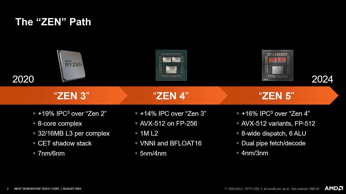
so AMD uses two Core complex(CCX) aka 8 Core Chiplets that are similar and binned differently that is one CCX can hit higher clocks and one CCX can't hit that high of a clock on one core they have different V/F curves . Here is how an AMD 8 Core Chiplets looks like. An AMD desktop CPU Contains 2 CCX and 1 IO Die containing IMC.The way Intel does Chiplets is not the same way AMD does CCD/CCX correct? AMD can add cores. Intel has a new chiplet.
Please correct me if I am wrong but I understood that to mean AMD has a whole next level of flexibility.
Here is a Zen 5 CPU with TWO CCX and IOD the problem arises when the core in one CCX has to access the data from another CCX it causes latency as the request has to route through IOD where the IMC lies to go from one CCX to another. This results in poor latency. Also i have added a curve for the different bins of Threadripper with 4 CCX.
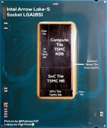
Now for Intel they also are based on similar principle they have an SoC die Containing IMC and a compute die containing the Cores but they only have a single Compute die or CCX in AMDs terms and a shared SoC die between different compute die.
The difference between AMD and Intel is Intel tapes out multiple compute die while AMD reuses the same CCX for all the Desktop SKU depending on binning and number of CCX but they tape out different dies for mobile.
Intel just uses two compute dies shared across Desktop and Mobile so for example ARL-H and ARL-S both share the 6+8 die while HX and S series share the 8+16 die with different SoC one with LP-E cores and one SoC without LP-E Cores. Of course there are different Binning for Mobile and Desktop. There is difference in Packing as well Intel uses exxpensive Foveros while AMD uses cheap packing.
Discussing AMD’s Zen 5 at Hot Chips 2024
Hot Chips isn’t just a conference where companies give in-depth presentations on the architectures behind high performance chips.
 chipsandcheese.com
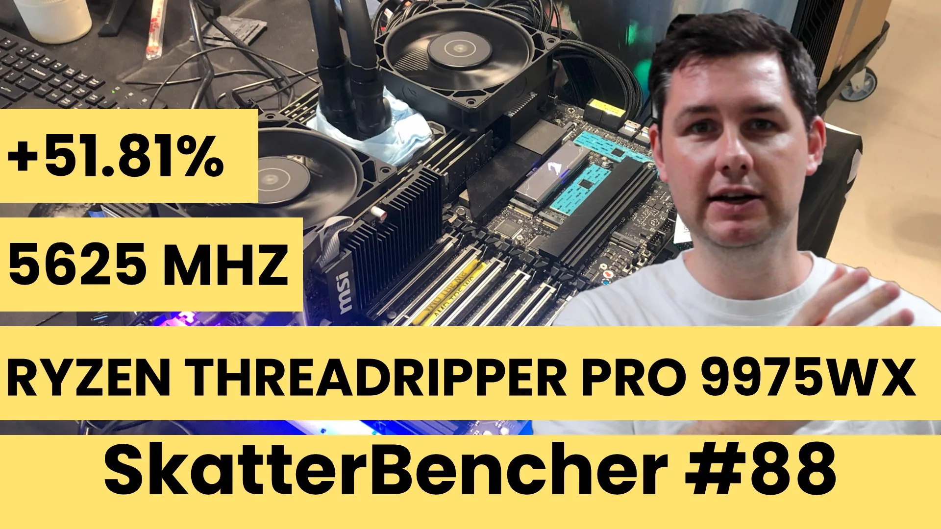
SkatterBencher #88: Ryzen Threadripper Pro 9975WX Overclocked to 5625 MHz - SkatterBencher
We overclock and undervolt the AMD Ryzen Threadripper Pro 9975WX to 5625 MHz with the ASUS Pro WS WRX90E-Sage SE and liquid cooling.
Attachments
No, it's notI think I asked you this before.
The way Intel does Chiplets is not the same way AMD does CCD/CCX correct? AMD can add cores. Intel has a new chiplet.
Please correct me if I am wrong but I understood that to mean AMD has a whole next level of flexibility.
It's just a difference in the concept of a chiplet
In terms of maturity, AMD is more mature
So what are the pros and cons of Intel chiplet implementation scheme vis a vis that of AMD's?Yeah but the DMs have no way to send Images so i couldn't explain properly
so AMD uses two Core complex(CCX) aka 8 Core Chiplets that are similar and binned differently that is one CCX can hit higher clocks and one CCX can't hit that high of a clock on one core they have different V/F curves . Here is how an AMD 8 Core Chiplets looks like. An AMD desktop CPU Contains 2 CCX and 1 IO Die containing IMC.
View attachment 3489View attachment 3488 View attachment 3490
Here is a Zen 5 CPU with TWO CCX and IOD the problem arises when the core in one CCX has to access the data from another CCX it causes latency as the request has to route through IOD where the IMC lies to go from one CCX to another. This results in poor latency. Also i have added a curve for the different bins of Threadripper with 4 CCX.
View attachment 3491
Now for Intel they also are based on similar principle they have an SoC die Containing IMC and a compute die containing the Cores but they only have a single Compute die or CCX in AMDs terms and a shared SoC die between different compute die.
View attachment 3493
The difference between AMD and Intel is Intel tapes out multiple compute die while AMD reuses the same CCX for all the Desktop SKU depending on binning and number of CCX but they tape out different dies for mobile.
Intel just uses two compute dies shared across Desktop and Mobile so for example ARL-H and ARL-S both share the 6+8 die while HX and S series share the 8+16 die with different SoC one with LP-E cores and one SoC without LP-E Cores. Of course there are different Binning for Mobile and Desktop. There is difference in Packing as well Intel uses exxpensive Foveros while AMD uses cheap packing.
Discussing AMD’s Zen 5 at Hot Chips 2024
Hot Chips isn’t just a conference where companies give in-depth presentations on the architectures behind high performance chips.SkatterBencher #88: Ryzen Threadripper Pro 9975WX Overclocked to 5625 MHz - SkatterBencher
We overclock and undervolt the AMD Ryzen Threadripper Pro 9975WX to 5625 MHz with the ASUS Pro WS WRX90E-Sage SE and liquid cooling.skatterbencher.com
Both have their advantages and disadvantages, but Intel can keep costs down by sharing parts with the most numbered laptop products.So what are the pros and cons of Intel chiplet implementation scheme vis a vis that of AMD's?
The disadvantage is that it is less mature than the AMD chiplet, since it has been in full swing.
The packaging costs are a bit more expensive than the AMD ones.
Well, if it's mass-produced, the cost issue may be offset.
It's just my opinion
siliconbruh999
Well-known member
AMDs biggest pro is binning and cost and IP ReuseSo what are the pros and cons of Intel chiplet implementation scheme vis a vis that of AMD's?
Intel's mostly is able to mix Match different IP so more combination is possible but not cost more chiplets cost more more so on different node's. Intel kind of botched their chiplet implementation as well