You are currently viewing SemiWiki as a guest which gives you limited access to the site. To view blog comments and experience other SemiWiki features you must be a registered member. Registration is fast, simple, and absolutely free so please, join our community today!
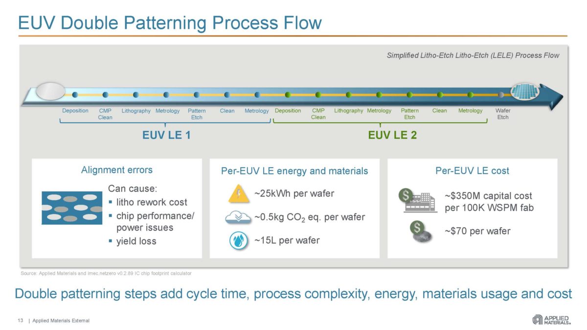
Applied Materials, Inc (NASDAQ: AMAT) showcased a patterning technology that helped chipmakers to create high-performance transistors and interconnect wiring with fewer EUV lithography steps, thereby lowering the cost, complexity, and environmental impact of advanced chipmaking. To help...
finance.yahoo.com
Any thoughts or observations on Sculpta machine would be appreciated, especially anyone that is planning on working with it.
I think the question may depending on the impact it can have in the industry. Will it make chip making a lot more affordable, so a lot more fabless companies can move to leading edge faster? or will the benefits eat away at Foundry level?
The SPIE Advanced Lithography Conference is the semiconductor industries premier conference on lithography. The 2023 conference was held the week of February 27th and at the conference Applied Materials announced their Sculpta® pattern shaping tool. Last week I had an opportunity to interview...
Sculpta, according to Applied's own claims, is useful for narrowing gaps in very specific kinds of pattern, allowing features drawn with a single EUV or ArFi exposure to avoid adjacent interference and then narrow the gap using a cheaper machine.
It looks like specific use cases might be boosted by EDA that can prepare the suitable geometry, but even so it hardly is a magic solution for all mask patterns. So it might reasonably be expected to save a minor fraction of EUV exposures, and that will depend upon how aggressively complex the designers like their patterns to be. Some might conclude that the greater flexibility of the patterns possible with dual exposure is a better choice.
Applied seems to have some launch customers. This kind of tech will require experience in the field to settle the question of how widely accepted it becomes.
The target pattern (a narrow gap) and the expected input (a small oval) are both notoriously stochastic and low on image-slope. It's noble but foolhardy for etch to take on a burden that's fundamentally limited by lithography.

 finance.yahoo.com