Array
(
    [content] => 
    [params] => Array
        (
            [0] => /forum/threads/intel-16nm-vs-10nm.17509/page-2
        )

    [addOns] => Array
        (
            [DL6/MLTP] => 13
            [Hampel/TimeZoneDebug] => 1000070
            [SV/ChangePostDate] => 2010200
            [SemiWiki/Newsletter] => 1000010
            [SemiWiki/WPMenu] => 1000010
            [SemiWiki/XPressExtend] => 1000010
            [ThemeHouse/XLink] => 1000970
            [ThemeHouse/XPress] => 1010570
            [XF] => 2021770
            [XFI] => 1050270
        )

    [wordpress] => /var/www/html
)

Intel 16nm vs 10nm?

If TSMC announces 16nm production in Arizona, then Intel will need to expand the number of 2x layers to 4, or hope that TSMC's MRAM doesn't work too well, correct? Is that the bottom line?

Edit: GF has an amazing opportunity here. GF should not be allowed to merge with TSMC, Intel, nor Samsung if they have received any USG funding.
 
Last edited:
Users in the non intelean world has choices of different threshold FETs. I will assume similar gains and leakages.
Not relevant. Like 10nm and beyond 22FFL uses different WF metals in the metal gate, allowing the fins to be undoped.
iedm-2017-intel-22ffl-short-channel-effect-768x265.png


Let me make sure I am reading this correctly.
M1 - M6 pitch = 1x = 90nm
M7-M8 = 12x = 1080nm

Is the 4000 the bump layer (API) or the layer below the bump?
iedm-2017-intel-22ffl-metal-stack-768x315.png

This picture shows that M8 is the first giant metal layer for the mim caps and power routing and is below the bump. Suppoisedly this is also where those monster inductors can be built.

What are the 0+ layers? Are these options? How many thick layers are we allowed to use?
Yeah those are optional layers. Based on the ieee whitepapers it seems they are pick and choose as many or as little as you want.

Do the transition vias (via67) require a large via or lots of small vias?
No clue that isn't in whitepapers and I don't design chips for 22FFL (or any node for that matter). I would assume lots of little vias since upper metals are generally supposed to be for global power routing, but I don't know for sure.

I am comparing your process this process (the world outside of Intel): 8 1x layers, 2 2x layers, 2 4x layers. I consider this to be 9 routing layers (M10 transition layer. Typically wide)

If we assume that users can use 2 2x (180nm) layers, then 22ffl are 2 layers short of competitor, correct?
I would suppose, the link you shared just said how many layers I could use on 12LPP and 16FF not what their pitches were. If you were okay using the 8x to then it would be 1 layer short. Either way it is not really my place to tell you what process node to use, I just didn't understand how you thought 22nm SOC could ever be considered better than intel 16. I have no clue how it compares to the 28nm metal stack, but even if it is a bit shorter than foundry 14nm, it should at least be cheaper due to the smaller stack height and no SADP/LELE.

Perhaps Intel is hiding what they will have available for IFS until after they get their Chips Act funding?
That strikes me as unlikely and counter to intel's goal of actually receiving funding.

Note: The contact us page didn't result it getting me any responses
Recently? Or are you still talking about your poor experiences from a year ago? All I can say is that I am in the camp of many on this forum that it will take years for IFS to be as good on the services/ecosystem front as GF and TSMC are. It took those firms decades to get to where they are today, and in the meantime there is a lot for IFS to learn to get those base competencies.
 
I did not understand the 0+. If the customer can choose four 2x layers, that would work. I doubt the customer can pick any number of thick layers they want.

I cannot disclose the pitches of Intel's competitors. Just like you, I can only state what is publicly available. 1x, 2x, etc works

I contacted Intel last week. No answer. Emailed VP and a couple of others in November. No reply.

Intel is not a new foundry. They came up with FINFETs before TSMC. Do you think that Andy Grove would find this timeline acceptable? Would he agree with you? Does TJ? It is clear to me that Intel doesn't want to deal with lots of foundry customers. They are focused on their proprietary CPU, FPGA, etc. IFS purpose is "hey, we got it anyway, we may as well let some of the big guys use it. Forget the little guys.

I just wanted to do my due diligence and determine what our next process will be. We will stick with TSMC and GF. I am happy with that.
 
I did not understand the 0+. If the customer can choose four 2x layers, that would work. I doubt the customer can pick any number of thick layers they want.
If your application requires such dense logic why don't you consider 8LPP? It offers far better cost per transistor than "14nm", doesn't require you to buy an expensive EUV mask set like N6/7LPP (probably important due to the low volumes your customers have), and offers much better PPW (around intel 16 levels).

I cannot disclose the pitches of Intel's competitors. Just like you, I can only state what is publicly available. 1x, 2x, etc works
Yeah I wasn't expecting you too. I was more so saying that if cost wise intel 16 is competitive with like 22FDX, then maybe comparing it to other 28nm processes in addition to 14nm processes makes sense. Based on how intel talks about it, it seems like intel 16 is targeted at low cost, analog/RF, and embedded applications rather than complicated HPC/AI things. But if that was a customer's goal I don't know why they wouldn't just use a newer node that is even cheaper on a transistor basis, uses less power, and has an even larger metal stack to work with.

Intel is not a new foundry. They came up with FINFETs before TSMC. Do you think that Andy Grove would find this timeline acceptable? Would he agree with you? Does TJ?
Foundry =/= fab cliff. Take for example Ajinomoto vs Chemours. They both make chemicals, but making and selling MSG is very different than high performance chemicals. Plant design, quality testing, how you run the production line, all of these things need to be different. Ajinmoto can focus on it's small product stack at excellent scale. Whereas Chemours needs to closely work with customers for the right chemical for their customer's processes, ensure it meets the specs that customer wants, and then produce this chemical at the agreed upon quality alongside the chemicals for all of their other clients. Obviously this is not one to one with how an IDM fab vs a foundry fab operate, but it gives you an idea of the scale of changes that need to happen for intel's internal foundry model transformation.

I just wanted to do my due diligence and determine what our next process will be. We will stick with TSMC and GF. I am happy with that.
Power to you. That is what all engineers should do. Investigate all options and roll with the best choice. It is so annoying when there is a cool or innovative products that people don't even consider because it isn't from their normal auto buy company. If intel 16 is not right for your customers, then you are under no obligation to buy it. Although in your case it seems they are making it easy for you by not letting you.
 
If your application requires such dense logic why don't you consider 8LPP? It offers far better cost per transistor than "14nm", doesn't require you to buy an expensive EUV mask set like N6/7LPP (probably important due to the low volumes your customers have), and offers much better PPW (around intel 16 levels).
Nice. Can you refer me to a site that provides the metal stack info. Does anybody make exotic RAM for it? Is it FINFET? Of course I need to ask, do you believe IFS will offer this as MWPs next year?

You should handle IFS marketing. I am serious. Customers will love you. Thanks!
 
Nice. Can you refer me to a site that provides the metal stack info. Does anybody make exotic RAM for it? Is it FINFET? Of course I need to ask, do you believe IFS will offer this as MWPs next year?
Samsung is far more insular on the technical details of their process technology that is available publicly. The fact that Samsung 8LPP is all the rage these days due to it being the second densest non EUV foundry process (N7/N7P being the densest non EUV node) does point to greatness though. Here is everything I could dig up.

https://ieeexplore.ieee.org/document/8510673

There also seems to be an 8LPU with a single fin library option and a new lower power ULVT.

Anandtech:
Screenshot_20230315_140052.png

(side note in case you didn't know 14LPP is identical to GF14LPP because they licensed it from Samsung)

Here is recent snapshot of their trailing edge roadmap.
ssf-17lvp-map_wc.png


They also have an enhanced version of their 14LPP that sounds very similar to GF12LPP in concept, and if density isn't a concern they have some FDSOI options. Since it seems US capacity is important to you, I thought it worth pointing out that Samsung has a pretty large 14/11LPP fab in Texas that also does their 32/28nm and 65/45nm tech.

As for when you will get an IFS MPW, 🤷‍♂️ I don't know man I'm just a chemical engineer.
 
I don't know why they wouldn't just use a newer node that is even cheaper on a transistor basis, uses less power, and has an even larger metal stack to work with.

I believe the price is higher per FET on triple patterned processes.

The Asianometry 7nm video is why I have avoided going below 16-12nm. I am certain everybody in the forum has seen it. I am told it is accurate. Is it? Was it?


We will stick with gf14, ts16, gf22, ts28. We believe this is the ASIC sweet spot.
 
I believe the price is higher per FET on triple patterned processes.
I professionally disagree. Even today the cost per FET keeps decreasing (although the rate of that decrease is slowing). I'm with Dan and Scotten on this one; people WAY over estimating what N5 and N3 wafer costs are. Of course depending on your exact design the results can get much worse. For example if you wanted to make a pure SRAM die on N3E instead of N5 yeah that would be a cost per FET increase because SRAM density did not scale between those nodes. Same deal with analog which also doesn't very well below "10/7nm" class nodes (at least per AMD). Speaking of AMD I don't think they would have started using the N7 family on their IO dies if the cost per FET increased for those nodes. The fact they moved price sensitive parts like those that don't even need the better PPW of N7 vs 12LPP is proof in the pudding that cost per FET still is decreasing. Heck even for the denser than N5 intel 4, intel has claimed that there was "a large cost per FET reduction versus intel 7" (no doubt off the back of EUV simplifying the process flow).

The Asianometry 7nm video is why I have avoided going below 16-12nm. I am certain everybody in the forum has seen it. I am told it is accurate. Is it? Was it?
But 16FF and 14LPP also have a restrictive design rules and double patterning. Why is it acceptable there but not for "10nm" class nodes like 10/8LPP or N7 family? If you are already used to unidirectional rules and double patterning, then shouldn't only a bit more double patterning not be that hard? 8LPP has LELELE, no SAQP, and the metals are also within the SADP regime. Additionally it is my understanding that Asianometry is wrong about N7's MP scheme. To my knowledge N7 does not have any LELELE. Just SADP for the metals and SAQP for the fins. I could be wrong, but I thought that for the most part the only thing designers really draw are the metals. With the fins just filling up a grid. Also I thought modern EDA abstracts much of the difficulty associated with MP?

We will stick with gf14, ts16, gf22, ts28. We believe this is the ASIC sweet spot.
It's your business, do what you think is best.
 
Per DK:

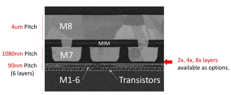
"Intel’s 22FFL metal stack is similar to a foundry SoC process and includes three novel layers. The metal layer pitches are all integer multiples and generally optimized for low-cost. Intel’s team chose a minimum pitch of 90nm for the lowest 6 layers. Unlike previous Intel process technologies, this metal 1X layer supports complex routing using only single-patterning lithography, eliminating a second exposure compared to the 22nm SoC process. Two thick metal upper layers are available for routing power and ground, and they are also used to form inductors and metal-insulator-metal capacitors. The 1080nm pitch metal layer is re-used from existing process flows, but the 4000nm pitch top metal layer is entirely new. In addition, the process flow supports optional 2X, 4X, and 8X pitch metal layers; the 720nm 8X pitch is also a new layer defined specifically for the 22FFL node.

Intel_22FFL_metal_stack.png

Table 1 – Metal layers for Intel’s 22nm SoC, 14nm SoC, and 22FFL process technologies.
* indicates uni-directional pitches.
‡ indicates multi-patterning.

Compared to 22nm SoC, the 22FFL metal interconnects are much easier for modern EDA tools. Supporting complex shapes in a large number of similar metal layers avoids restrictive design rules and splitting shapes across multiple layers, which enables automated tools to generate denser layouts. This is particularly important for foundry customers, which are not familiar with Intel’s highly restrictive design rules, and for ASIC-like designs (e.g., modems) where clock frequency does not directly translate into value. In contrast, the tapered interconnect hierarchy for the 22nm and 14nm nodes can achieve higher performance, but only by carefully taking advantage of the unique characteristics of each layer, which is difficult for automated tools."

From some digging the 22nm SOC BEOL:
iu

It seems back then what is now called M0 was called M1. That or in intel jargon TCNs are M0, but I have yet to find a clear answer for this floating around the web.

Sorry it isn't a ticket onto a MPW or what the exact options are on i16, but this is what I can find floating around the web. It at least seems to be about as detailed as those europractice GF and TSMC public numbers. But it is obviously less detailed than the full PDKs you already have.
I'm not sure this is true these days : "In contrast, the tapered interconnect hierarchy for the 22nm and 14nm nodes can achieve higher performance, but only by carefully taking advantage of the unique characteristics of each layer, which is difficult for automated tools."

Place and route tools have had smart layer promotion to take advantage of modern layer stacks which offer 3 (or perhaps more now) widths of standard routing layers. Not least because this was required for Intel's more advanced processes. I'm sure I recall reading articles about Synopsys and Intel on this very subject several years ago.
 
On the topic of 7nm, what and when by whom I was told was consistent with that video. Maybe we had the same source? Our clear conclusion was 16/12, and that is our last PDK we will support on DUV. Yes, it was off the charts difficult. Took many years to automate. Customers would have to pay us to automate 7.

There was article posting on a semiwiki thread, perhaps by Fred, that showed the following mask set prices:

28nm = $3M
16nm = $5M (winner. see below)
5nm = $15M
3nm = $20M

If somebody can update these numbers, including a 7nm DUV only, please do so.

Our SerDes, which includes signal driven split up PLLs, was reduced in size by a factor of 3 when migrating from 28nm down to 16nm. Our own standard cells that were designed to withstand 1.5v connections were used. We cheated on the pads, I/O protection and bandgap by making them smaller. I can believe the 3x FET count increase from another document that was added to semiwiki thread. Couple that with the increased efficiency and reduced leakage of finfets makes a 28 => 16nm appealing. Add an eFPGA on top of that, then it is a no-brainer. Note: Exotic RAM and I/O counts for HBM or PICs is a major variable that can change conclusions.

I am assuming $15M mask costs for 5nm will be a no-go. This is pure speculation. I don't know if those numbers are still valid.

Note: We use our own place and route tools.
As I am sure you are well aware mask set costs =/= wafer cost. As the number of layers increase mask costs will increase linearly. EUV replacing multi patterning layers can reduce mask count, but there are also situations where it can increase costs due to the larger per mask cost. Obviously if you are doing large production runs, not a big deal either way and you want to move to new nodes as fast as is reasonable on the foundries yield/depreciation curve. But since your customers are doing low volume ASICs, it is probably hard to justify the cost of the mask set on an EUV node. N7P is all optical, and the multipatterning there isn't much more complicated then what you already worked on. Combine this with the large PPW improvement and more than tipple the density of 16FF. The benefits seem well worth the little bit of extra work over 16FF. I can also guarantee you that N7P does not cost more more than triple 16FF (especially now that fabs should be fully deprecated by now).

8LPP is obviously a whole nother can of worms since you would have to learn to deal with LELELE. But the mask count should be even smaller than N7P while still offering full node scaling over GF's 14/12LPP for not a huge uptick in cost. Combine that with Samsung's low mark-up and you will probably get a really good deal.
 
Thank you. You read me loud and clear. I don't care about recurring cost. It's ASIC vs FPGA. That's it. Note: I like eFPGAs. Prove your RTL in FPGAs, then hard code most of it in an ASIC if volumes, power, size justify it.

As I am sure you are well aware mask set costs =/= wafer cost
I learned that from you guys on semiwiki. I love that simple formula!

N7P: Can you break it down and estimate on your predictions of 2026 feature and costs?
What exotic memory and at what voltage?
SRAM size savings?
Standard cell size savings?

I understand that you don't have a crystal ball, but neither do I. I make decisions based on speculations. A this point, I am use the tick-toc strategy of handling the PDK and automation, then making the IP. I was going to go to the "tick" with IFS, but I gave up on that last week. We will push the Tick to till next year. I guess the choice will be N7P if you convince me, else AZ-5nm
 
Thank you. You read me loud and clear. I don't care about recurring cost. It's ASIC vs FPGA. That's it. Note: I like eFPGAs. Prove your RTL in FPGAs, then hard code most of it in an ASIC if volumes, power, size justify it.


I learned that from you guys on semiwiki. I love that simple formula!
np

N7P: Can you break it down and estimate on your predictions of 2026 feature and costs?
Hard to say. TSMC is mostly pushing N6/N6-RF for their speciality tech because of the lower cost per FET and wanting to make their money back on those EUV machines they bought for Apple fon N7+. N7P might be kind of slim for the stuff that isn't used for mobile/HPC. I would dig around the articles for the TSMC category, as there are tons of ecosystem updates for TSMC.

What exotic memory and at what voltage?
I think I saw that there were plans for N6-RF to get that sort of stuff, but I don't know for sure.

SRAM size savings?
2.7x HD SRAM density

Standard cell size savings?
I don't know the exact dimensions for 16FF. But per teardowns the HD N7/NP is 240x57 and the HP is 300x64. Min metal pitch is 40nm, min gate is 57nm, and min fin is 30nm.

I understand that you don't have a crystal ball, but neither do I. I make decisions based on speculations. A this point, I am use the tick-toc strategy of handling the PDK and automation, then making the IP. I was going to go to the "tick" with IFS, but I gave up on that last week. We will push the Tick to till next year. I guess the choice will be N7P if you convince me, else AZ-5nm
Can't you just ask TSMC for that info since you already seem to have a good relationship going there? They could also give you far better answers than I could ever give. Based on that response I also assume Samsung that 14/11LPP and 8LPP are out of the running. A bit of a shame, as I have a bit of a soft spot for IBM/GF/Samsung, but at the end of the day it is no skin off my nose.
 
Companies with $50M bank accounts (should be spread across 200 banks, else you are an irresponsible CEO) have better relationships.

So N6 uses EUV. Is M4 double patterned?

Does HD = high density and HP = high performance?
Min metal pitch is 40nm, min gate is 57nm, and min fin is 30nm.

To be clear, the M2 pitch is 40nm?, the min gate pitch = 57nm, and fin pitch = 30nm. This sounds consistent. Can you tell me what the M4 (double patterned) and M5 pitch is? 60nm would make sense, and a gate pitch of 60nm might be allowed, physics depending. I would be more interested in high performance, if HP means that.

I never heard of N6. I think you just defined our tick!
 
So N6 uses EUV. Is M4 double patterned?
correct

Does HD = high density and HP = high performance?
yes

To be clear, the M2 pitch is 40nm?, the min gate pitch = 57nm, and fin pitch = 30nm. This sounds consistent.
yup

Can you tell me what the M4 (double patterned) and M5 pitch is? 60nm would make sense, and a gate pitch of 60nm might be allowed, physics depending. I would be more interested in high performance, if HP means that.
Per wikichip: M4 is 40nm M5 is 76nm single patterned unidirectional. Per Qualcomm when they used the HP library for one of their big cores they saw around a 10% drive improvement at slightly increased leakage. Per TSMC N7P was +7% performance or -10% power over N7.

I never heard of N6. I think you just defined our tick!
It is design rule compatible with N7/N7P and offered single dummy gate isolation and EUV for process simplification.
 
Maybe not. I forgot about the $50M rule. Can somebody give us a $50M 1-day loan? Hopefully there won't be a bank run that day.
 
Back
Top