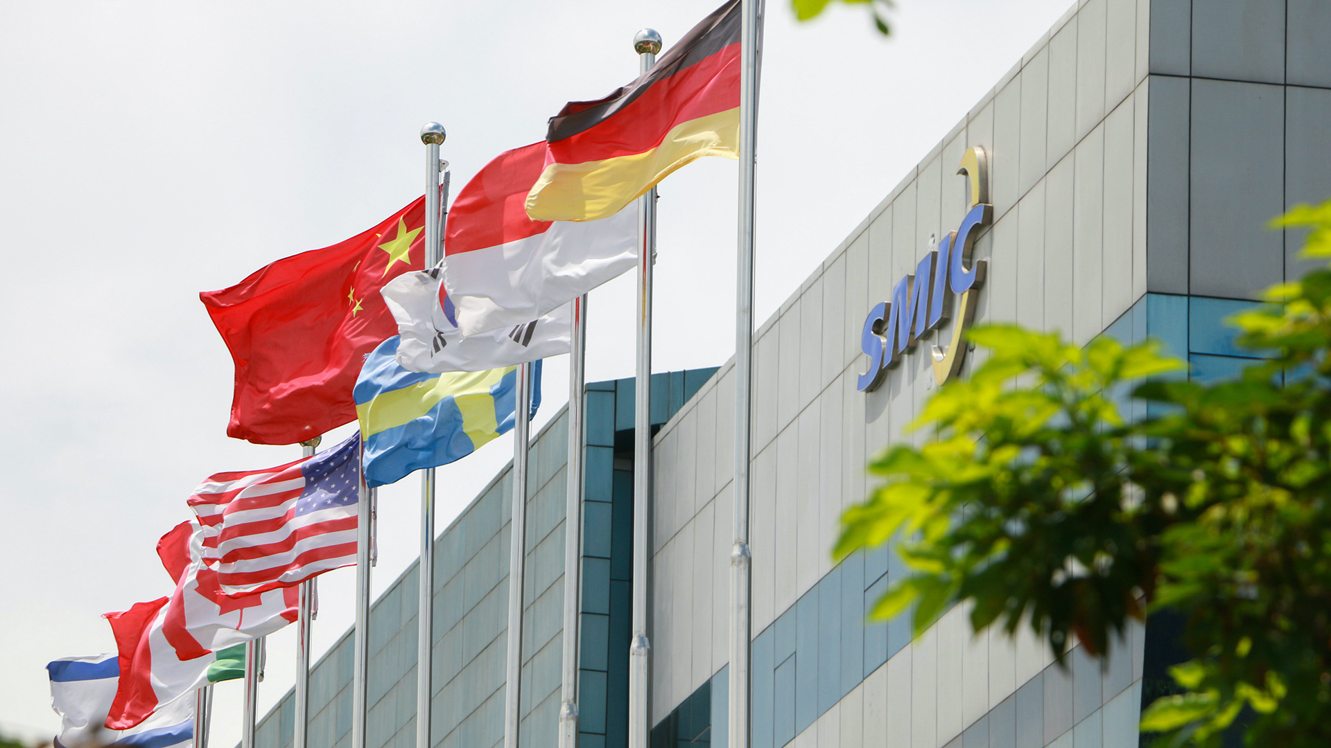
China's largest foundry SMIC to start full-scale 5nm operation next year; lack of essential equipment such as EUV… 5nm yield expected to be around 30% “SMIC's 5nm process price likely to be 50% more expensive than TSMC”
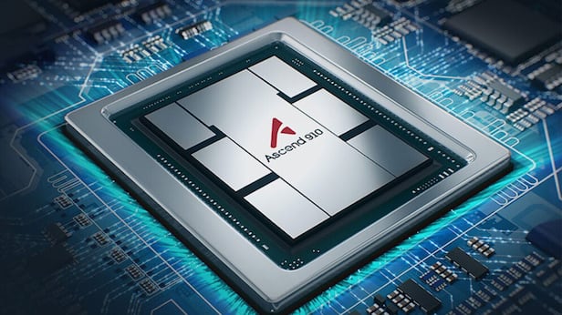
Huawei Ascend AI chip./Huawei
It has been reported that Huawei is providing full support to China's largest foundry (semiconductor contract manufacturing) SMIC for the successful mass production of the 5㎚ (nanometer, one billionth of a meter) process scheduled for operation next year. As the advanced processes of TSMC and Samsung Electronics cannot be utilized due to US regulations, it seems that Huawei is tightening the reins on cooperation such as equipment development so that SMIC, a domestic company, can stabilize the 5㎚ process.
According to industry sources on the 1st, SMIC plans to start operating the foundry 5㎚ process next year. SMIC plans to complete the mass production line by introducing the equipment necessary for mass production of the 5㎚ process as early as this year. SMIC, like Huawei, is subject to US regulations, and imports of ASML's extreme ultraviolet (EUV) exposure equipment, a key facility for processes below 7㎚, are restricted, making it difficult to develop advanced processes.
◇ Huawei's latest AI accelerator manufactured with SMIC 7nm
Huawei recently unveiled the AI accelerator Ascend 910C. The Ascend 910C is an AI accelerator specialized in inference, and has been evaluated to surpass Nvidia's advanced AI accelerator H100 in inference performance. The Ascend 910C will be used by Chinese IT companies, including DeepSec, to develop AI models. The Ascend 910C is known to have been mass-produced using SMIC's 7nm process.
There is a prevailing view that Huawei's mass production of next-generation AI chips will be hindered as SMIC's advanced process is still at the 7㎚ level. Currently, Nvidia, AMD, Intel, etc. are manufacturing AI chips using TSMC's advanced process of 3㎚ or less, so in order to compete with them, it is essential to apply a fine process that can improve chip performance.
To this end, Huawei is understood to be risking its life to ensure smooth mass production of the 5㎚ process of SMIC, a domestic foundry company. Chinese semiconductor equipment company 'SciCarrier', known to be developing equipment in cooperation with Huawei, unveiled a number of equipment solutions applicable to fine processes at SEMICON China 2025 last week. The company is known to have registered a patent for a deep ultraviolet (DUV) equipment process that can replace EUV exposure equipment in the 5㎚ process . In addition, Huawei is said to be strengthening cooperation with SMIC, such as process optimization, so that it can maximize the performance of its chips.
The Hong Kong South China Morning Post (SCMP) reported that “Psycarrier registered a patent two years ago to manufacture 5nm semiconductors using DUV equipment. This is also related to SMIC using DUV to manufacture Huawei’s application processor (AP) using a 7nm process.”
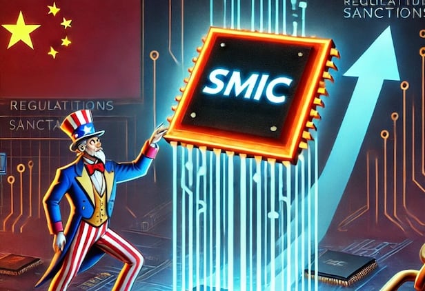
◇ SMIC 5㎚ yield around 30%… “Factory price will be 50% more expensive than TSMC”
The problem is that when using DUV equipment, the precision is lower than that of EUV equipment, resulting in lower yields. If DUV is used instead of EUV, there is a disadvantage in that the semiconductor photo paper position must be adjusted and light must be projected multiple times. Normally, when EUV is used in the 5㎚ manufacturing process, the exposure process is repeated once, or at most twice, but when DUV is used instead, it must be repeated at least four times. As the process becomes more complicated, the yield is bound to become unstable, and the performance of the semiconductor is likely to deteriorate.
Park Yoo-ak, a researcher at Kiwoom Securities, said, “SMIC’s 5㎚ process yield is expected to be less than one-third of that,” and “Due to the low yield, the price of the 5㎚ process is also expected to be 50% more expensive than TSMC.” Currently, TSMC’s 5㎚ process yield is over 90%, while SMIC’s 5㎚ process yield is expected to be around 30%.
A semiconductor industry insider said, “The prevailing analysis is that SMIC’s 5㎚ process yield and performance will fall far short of TSMC and Samsung Electronics’ processes,” but added, “If the process stabilizes thanks to domestic semiconductor manufacturing demand and the level of Chinese semiconductor equipment companies improves, they can quickly increase their market share, which poses a threat to competitors.”

 biz.chosun.com

Huawei Ascend AI chip./Huawei
It has been reported that Huawei is providing full support to China's largest foundry (semiconductor contract manufacturing) SMIC for the successful mass production of the 5㎚ (nanometer, one billionth of a meter) process scheduled for operation next year. As the advanced processes of TSMC and Samsung Electronics cannot be utilized due to US regulations, it seems that Huawei is tightening the reins on cooperation such as equipment development so that SMIC, a domestic company, can stabilize the 5㎚ process.
According to industry sources on the 1st, SMIC plans to start operating the foundry 5㎚ process next year. SMIC plans to complete the mass production line by introducing the equipment necessary for mass production of the 5㎚ process as early as this year. SMIC, like Huawei, is subject to US regulations, and imports of ASML's extreme ultraviolet (EUV) exposure equipment, a key facility for processes below 7㎚, are restricted, making it difficult to develop advanced processes.
◇ Huawei's latest AI accelerator manufactured with SMIC 7nm
Huawei recently unveiled the AI accelerator Ascend 910C. The Ascend 910C is an AI accelerator specialized in inference, and has been evaluated to surpass Nvidia's advanced AI accelerator H100 in inference performance. The Ascend 910C will be used by Chinese IT companies, including DeepSec, to develop AI models. The Ascend 910C is known to have been mass-produced using SMIC's 7nm process.
There is a prevailing view that Huawei's mass production of next-generation AI chips will be hindered as SMIC's advanced process is still at the 7㎚ level. Currently, Nvidia, AMD, Intel, etc. are manufacturing AI chips using TSMC's advanced process of 3㎚ or less, so in order to compete with them, it is essential to apply a fine process that can improve chip performance.
To this end, Huawei is understood to be risking its life to ensure smooth mass production of the 5㎚ process of SMIC, a domestic foundry company. Chinese semiconductor equipment company 'SciCarrier', known to be developing equipment in cooperation with Huawei, unveiled a number of equipment solutions applicable to fine processes at SEMICON China 2025 last week. The company is known to have registered a patent for a deep ultraviolet (DUV) equipment process that can replace EUV exposure equipment in the 5㎚ process . In addition, Huawei is said to be strengthening cooperation with SMIC, such as process optimization, so that it can maximize the performance of its chips.
The Hong Kong South China Morning Post (SCMP) reported that “Psycarrier registered a patent two years ago to manufacture 5nm semiconductors using DUV equipment. This is also related to SMIC using DUV to manufacture Huawei’s application processor (AP) using a 7nm process.”

◇ SMIC 5㎚ yield around 30%… “Factory price will be 50% more expensive than TSMC”
The problem is that when using DUV equipment, the precision is lower than that of EUV equipment, resulting in lower yields. If DUV is used instead of EUV, there is a disadvantage in that the semiconductor photo paper position must be adjusted and light must be projected multiple times. Normally, when EUV is used in the 5㎚ manufacturing process, the exposure process is repeated once, or at most twice, but when DUV is used instead, it must be repeated at least four times. As the process becomes more complicated, the yield is bound to become unstable, and the performance of the semiconductor is likely to deteriorate.
Park Yoo-ak, a researcher at Kiwoom Securities, said, “SMIC’s 5㎚ process yield is expected to be less than one-third of that,” and “Due to the low yield, the price of the 5㎚ process is also expected to be 50% more expensive than TSMC.” Currently, TSMC’s 5㎚ process yield is over 90%, while SMIC’s 5㎚ process yield is expected to be around 30%.
A semiconductor industry insider said, “The prevailing analysis is that SMIC’s 5㎚ process yield and performance will fall far short of TSMC and Samsung Electronics’ processes,” but added, “If the process stabilizes thanks to domestic semiconductor manufacturing demand and the level of Chinese semiconductor equipment companies improves, they can quickly increase their market share, which poses a threat to competitors.”

中 반도체 굴기 선봉장 화웨이… 내년 SMIC 5나노 양산에 ‘사활’
中 반도체 굴기 선봉장 화웨이 내년 SMIC 5나노 양산에 사활 中 최대 파운드리 SMIC, 내년 5나노 본격 가동 예정 EUV 등 필수 장비 부족 5나노 수율 30% 안팎 전망 SMIC 5나노 공정 가격 TSMC보다 50% 비쌀 듯

