Array
(
    [content] => 
    [params] => Array
        (
            [0] => /forum/threads/huawei-issued-new-patent-to-enhance-chip-wafer-alignment-efficiency.19368/
        )

    [addOns] => Array
        (
            [DL6/MLTP] => 13
            [Hampel/TimeZoneDebug] => 1000070
            [SV/ChangePostDate] => 2010200
            [SemiWiki/Newsletter] => 1000010
            [SemiWiki/WPMenu] => 1000010
            [SemiWiki/XPressExtend] => 1000010
            [ThemeHouse/XLink] => 1000970
            [ThemeHouse/XPress] => 1010570
            [XF] => 2021770
            [XFI] => 1050270
        )

    [wordpress] => /var/www/html
)

Huawei issued new patent to enhance chip wafer alignment efficiency

Daniel Nenni

Admin
Staff member
Huawei Patent wafer alignment efficiency


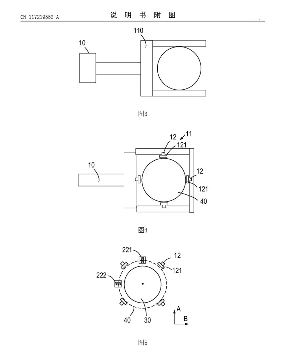
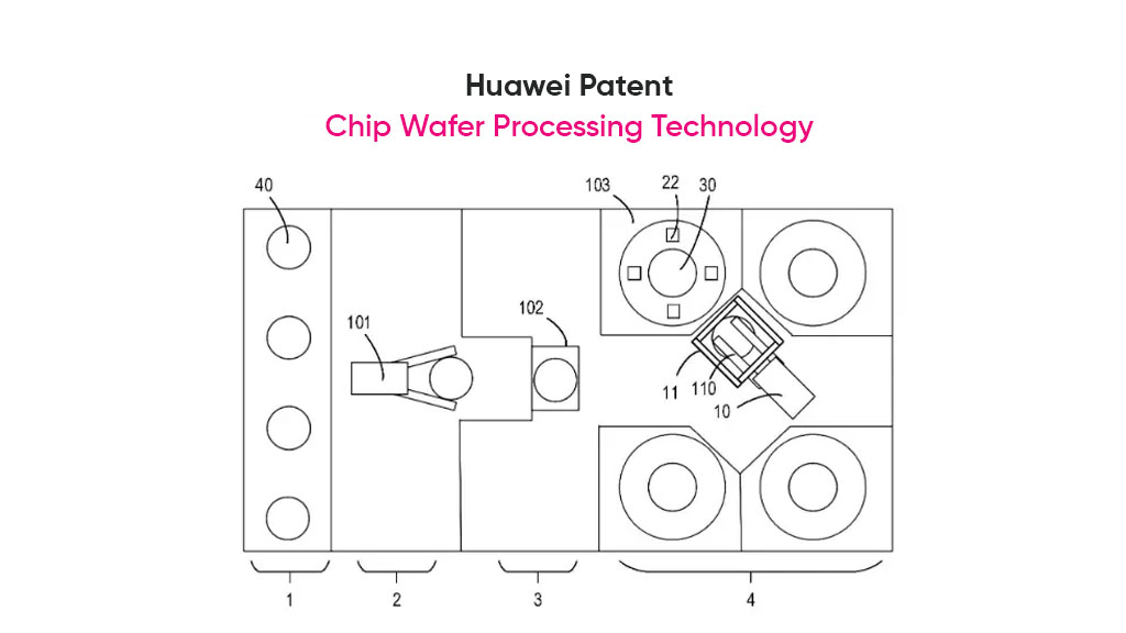
Huawei has applied for a new patent in the chip wafer processing technology to enhance the wafer alignment efficiency. The patent is entitled ‘Wafer Processing Device and Wafer Processing Method’ with an application number CN117219552A.

Huawei is already in rumors for building its own chip wafer fab manufacturing with the help of SMIC. Meanwhile, the new patent stamps confirmation and suggests that these speculations may turn out to be true in the time ahead.

Speaking of the patent application, Huawei focuses on improving the chip wafer alignment efficiency and accuracy. It further shows a list of equipment required in the wafer processing. Eventually, the wafer processing device counts:
  • Wafer carrier that can spin around the rotation axis
  • Mechanical arm with robotic hands to handle and place wafers on the carrier
  • Controller
  • Calibration component
Huawei Patent wafer alignment efficiency

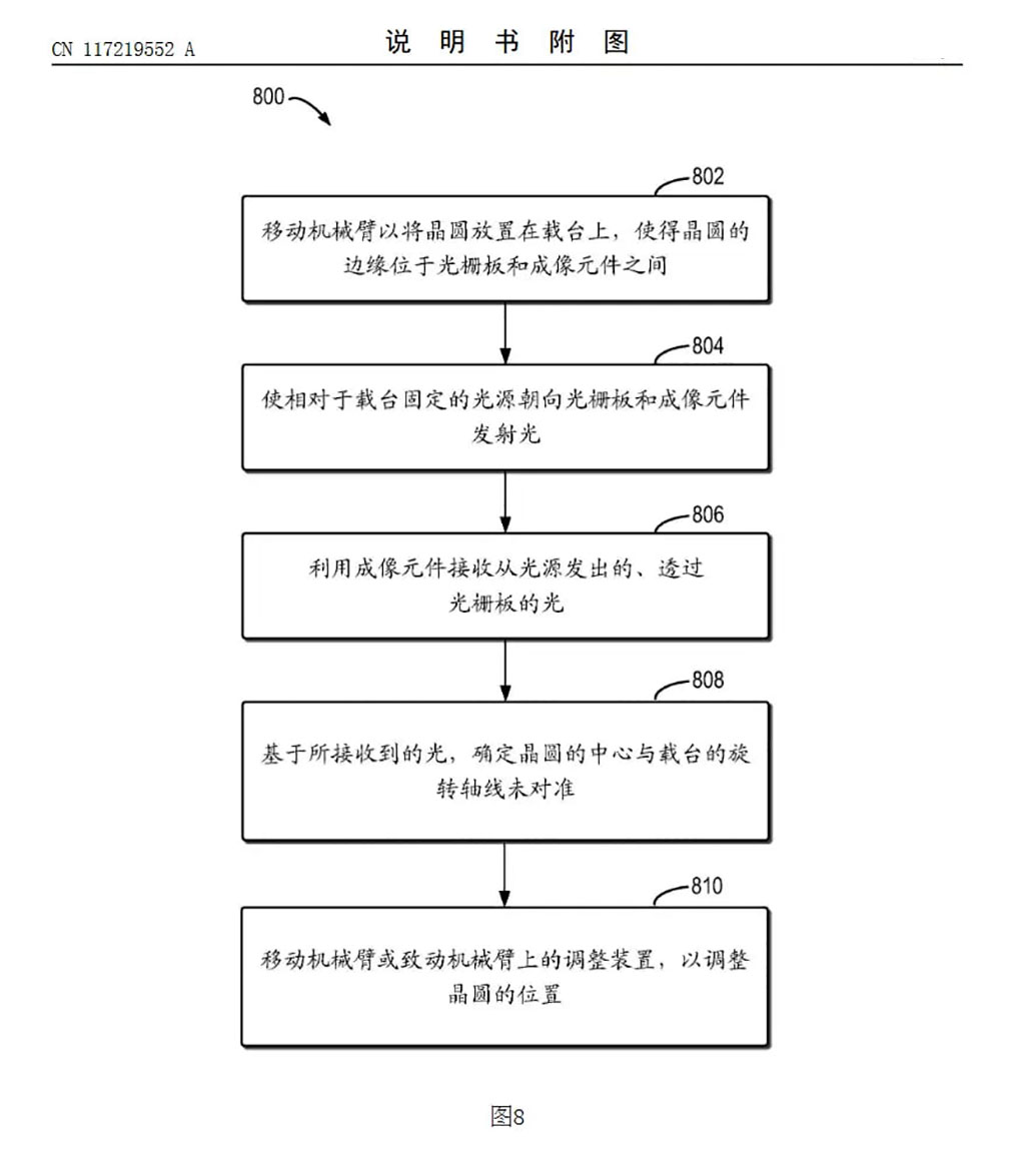
The calibration component includes a grating plate fixed relative to the carrier, a light source fixed to the grating plate, and an imaging element on the mechanical arm to receive light from the source, transmitted via the grating plate.

Meanwhile, the controller handles the mechanical arm and adjusts the position of the wafer, depending on the light detection by the imaging element. Now let’s look at the functioning aspects.

The grating plate and imaging element rest on opposite sides of the plane where the upper surface of the wafer carrier is located. Consequently, when the carrier holds the wafer, the grating plate and imaging element along with the upper surface help to carry the wafer and conduct processing.

Together, these devices and methods aim to improve wafer alignment efficiency and precision. As per the previous report, Huawei is likely to establish a wafer fab manufacturing factory in Shenzhen to meet the company’s requirements, and the respective patent shows the beginning of a new project.
Huawei Patent wafer alignment efficiency

 
Somehow improved alignment for a wafer handling robot is going to be key for Huawei building their own fab?
 
Huawei Patent wafer alignment efficiency


Huawei has applied for a new patent in the chip wafer processing technology to enhance the wafer alignment efficiency. The patent is entitled ‘Wafer Processing Device and Wafer Processing Method’ with an application number CN117219552A.

Huawei is already in rumors for building its own chip wafer fab manufacturing with the help of SMIC. Meanwhile, the new patent stamps confirmation and suggests that these speculations may turn out to be true in the time ahead.

Speaking of the patent application, Huawei focuses on improving the chip wafer alignment efficiency and accuracy. It further shows a list of equipment required in the wafer processing. Eventually, the wafer processing device counts:
  • Wafer carrier that can spin around the rotation axis
  • Mechanical arm with robotic hands to handle and place wafers on the carrier
  • Controller
  • Calibration component
Huawei Patent wafer alignment efficiency

The calibration component includes a grating plate fixed relative to the carrier, a light source fixed to the grating plate, and an imaging element on the mechanical arm to receive light from the source, transmitted via the grating plate.

Meanwhile, the controller handles the mechanical arm and adjusts the position of the wafer, depending on the light detection by the imaging element. Now let’s look at the functioning aspects.

The grating plate and imaging element rest on opposite sides of the plane where the upper surface of the wafer carrier is located. Consequently, when the carrier holds the wafer, the grating plate and imaging element along with the upper surface help to carry the wafer and conduct processing.

Together, these devices and methods aim to improve wafer alignment efficiency and precision. As per the previous report, Huawei is likely to establish a wafer fab manufacturing factory in Shenzhen to meet the company’s requirements, and the respective patent shows the beginning of a new project.
Huawei Patent wafer alignment efficiency

Will it be a very critical patent to be discussed? Which node this patent fits?
My opinion, it is general process equipment patent. The scale for wafer center shift will be um or sub um range, not the 2-3nm overlay or EPE control. Will China be restricted to get the solution for centering shift issue now? It should be not. It is not critical, and I would suggest not spending time on this.
 
Efficient chip wafer alignment is such a crucial part of tech advancements. I remember visiting a tech expo a couple of years ago where they showcased a wafer process demo—it was amazing to see how precise and intricate the work is. The way those wafers were aligned and processed really stuck with me, especially when they explained how even a tiny misalignment can cause massive issues down the line.

Huawei’s new patent could be a game-changer in making this process even smoother. I can’t help but wonder how it might influence production times or even reduce costs for end products. Innovations like these remind me how much goes on behind the scenes in the tech we use daily.
 
Last edited:
I'm not sure I understand why you've posted this patent on the forum. Are you trying to show that SMIC and Huawei work together, or are you just joking about this patent?
 
Huawei’s new patent could be a game-changer in making this process even smoother. I can’t help but wonder how it might influence production times or even reduce costs for end products. Innovations like these remind me how much goes on behind the scenes in the tech we use daily.
It was clear a year ago when this thread was active that this patent isn't important. You should have let it lie dormant.
 
Back
Top