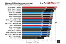
The one on Arrow lake clearly illustrate the point that Intel design team can no longer use manufacturing as an excuse. They are using TSMC N3B., yet failed to deliver a good score even company to last gen AMD product 7850X3D, and mediocre compare to current gen non-X3D product.
and an environment with or without internal fabrication constraints, are clearly different.
They are working with TSMC, and I don't think they need to worry much about internal fabrication constraints. The current gen microarchitecture was designed to be >99% compatible between PDKs.
And here is the thing. As an Intel investor here, when they are doing a good job, I feel very proud. But if they aren't, I can speak truthfully. And so far, they hasn't. I don't have to be an engineer to understand how disappoint the professional feels when they are testing the real silicon. I see it from their thumbnails. And they shouldn't have done it this poorly.
The design team must be hold accountable.
In 2005, if Paul Otellini had convinced the board to buy Nvidia, the designers would have had a totally different environment, and likely a wider scope of talent, all of which would have improved said designers.
In tech, literally no one should do M&A unless you are going for the market. But if you aren't a good capital allocator, then you shouldn't be thinking of it at all.
Even if Paul O acquired Nvidia. He could do very little to change the upside. There will be Avidia or Ovidia in the market eating Intel's lunch just like what's happening today. There's nothing that could be done, little they can save because they are poor allocators. Every investment they have made over the last 20 years have turned out to be an disaster. This includes every acquistion they did, see mobileye, habana, altera, etc. Hundred of billions of USD worth of stock being repurchased. None actually boost it significantly, because they don't have a proper business model.
I see you are still trying to be obtuse
Intel's and Andy Grove's biggest mistake was not having the right successor and executive team to continue his mantra "Only the paranoid survive." Having the right culture is everything and with the technical world advancing at an ever-accelerating rate, there is less and less time and room for...
semiwiki.com
And here is the thing. Gelsinger is not wrong, he is paranoid, otherwise they aren't going to go through this difficult path at first place.
Yet, it is worthy to be tried.