You are currently viewing SemiWiki as a guest which gives you limited access to the site. To view blog comments and experience other SemiWiki features you must be a registered member. Registration is fast, simple, and absolutely free so please, join our community today!
A roadmap from a group based in Shanghai published a paper with CSTIC 2023, showing a roadmap to 1nm, with the post-FinFET coming in at 3nm. The focus of the paper, however, was visualizing how to do 5nm without EUV. Their 5nm model is ~30 nm minimum metal pitch and ~50 nm gate pitch. As expected, substantial multipatterning would be needed, up to 6 masks on some layers (I estimated ~80 masks just for all the multipatterning only!). Their biggest concerns are CD and overlay control, for some short rectangular features. In particular, the biggest burden are the line cuts, which in their present scheme is not (totally) self-aligned.
Yer, they can reach 5nm, even 3nm is not impossible, but the yield, and manufacturing cost associated with nodes without EUV would be tremendously high, and infeasible for large scale production.
It nonetheless would be a fantastic propaganda tool for the CCP government against the USA, and its critics.
With EUV, multipatterning was already necessary at 5nm, it wouldn't be a surprise for them to be comparable. You could have 6 masks DUV SALELE + 4 cuts vs. 4 masks EUV SALELE + 2 cuts.
I point you all to the intel 4 paper which has similar pitches to a hypothetical SMIC 5nm. They said without EUV mask layers or mask counts (I don’t remember) would increase 30% over intel 7. As a result I would have to assume that defect density and wafer cost on SMIC 5 would be crazy high.
I point you all to the intel 4 paper which has similar pitches to a hypothetical SMIC 5nm. They said without EUV mask layers or mask counts (I don’t remember) would increase 30% over intel 7. As a result I would have to assume that defect density and wafer cost on SMIC 5 would be crazy high.
Yer, they can reach 5nm, even 3nm is not impossible, but the yield, and manufacturing cost associated with nodes without EUV would be tremendously high, and infeasible for large scale production.
It nonetheless would be a fantastic propaganda tool for the CCP government against the USA, and its critics.
I point you all to the intel 4 paper which has similar pitches to a hypothetical SMIC 5nm. They said without EUV mask layers or mask counts (I don’t remember) would increase 30% over intel 7. As a result I would have to assume that defect density and wafer cost on SMIC 5 would be crazy high.
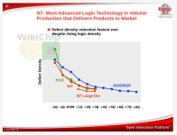
The increasing cost trend is unavoidable but the expected yield/defect risk from having more mask steps by itself seems disproven by none other than TSMC:
To me, what this shows is increasing process capability and better integration to make up for higher process complexity. Obviously there is no way to know what parts of a given node that TSMC had to work the hardest to get working; but it is possible that this plot is just showing TSMC becoming better at applying MP techniques or getting to grips with finFETs. Either way all else being equal, more process steps will always lead to more defects (even if you can get each of the added steps to a very low number of added defects). All else NOT being equal, it is of course it is always possible for a flow with a large number of steps with low defects per step to beat a shorter flow with more defects per step (23nm metal paterning with direct EUV vs SALELE is an easy example). Additionally this plot does not show DD at the beginning of TD nor absolute values which I feel would be a key parts for this discussion.
Given the limited public data to work with I suppose the N7 vs N5 DD trend immediately before HVM readiness also acts as a counter point (even if I don't really like these plots due to the unknowns I listed).