You are currently viewing SemiWiki as a guest which gives you limited access to the site. To view blog comments and experience other SemiWiki features you must be a registered member. Registration is fast, simple, and absolutely free so please, join our community today!
No, it is a coherent memory bus. Nvidia include a vestigial PCIe capability for the little bit of IO they care about. NVLink is more like an extended system fabric where switches and NICs are participants inside the fabric.
Not unless they screw it up. And some of the reports say it is based on extending AMD Infiniband, which properly puts it in the system fabric category, not the IO category.
Intel was fundamentally wrong to try to overlay system functionality on PCIe with CXL. They tried to work around that with tricks like mode 3 for CXL.mem which bypasses the archaic IO stack, but the correct way to do it is to extend the system bus over low latency links and then if you want old-fashioned IO put it behind an offload block.
Are you talking about AMD's Infinity Fabric? That's not InfiniBand. I also never believe "some reports". As for Intel's CXL design, it uses a different transaction layer than PCIe, and only the PCIe PHY is common. Both transaction layers are peers above a layer that can interleave them, called "Flex Bus". See page 33 of the CXL 2.0 spec.
Yes. I should proofread better. Are the reports accurate? I dunno. But I have reason to believe AMD are motivated to extent Infinity Fabric and have been looking at the options for a while.
As for Intel's CXL design, it uses a different transaction layer than PCIe, and only the PCIe PHY is common. Both transaction layers are peers above a layer that can interleave them, called "Flex Bus". See page 33 of the CXL 2.0 spec.
Yah but the modes 1 and 2 for IO and for Coherence/Cache are tall messy stacks and mode 1 is essentially a repeat of the PCIe stack. Anyway, I think we both agree PCIe is trailing edge compatibility. CXL had some good ideas, but AI (properly) moved the goalposts to another county.
Intel's direction on CXL was blunted by their inability to deliver new silicon plus the unusable reality of 3D Xpoint which was the main goal of CXL.mem.
UALink is a critical item by a bunch of companies still quite alive and able to deliver, with a clear goal (NVLink compete) in sight. I doubt they will allow distractions.
GPU-to-GPU I/O exists on NVLinks, and NVLink appears to use a form of RDMA to allow GPUs to access each other's memories at the physical address level, but I've seen no evidence there is cache coherency on standard NVLinks. One data point, IBM's Power CPUs supported NVLinks directly on previous implementations, and there's no evidence I see of coherency traffic in IBM's implementation.
It occurred to me while I laying in a hotel bed in San Diego a couple of nights ago that there is indeed a version of NVLink, called NVLink-C2C, which is used for inter-processor cache coherency in Grace Hooper, and that was perhaps what you were thinking about. Read what Nvidia is willing to say about either version of NVLink here:
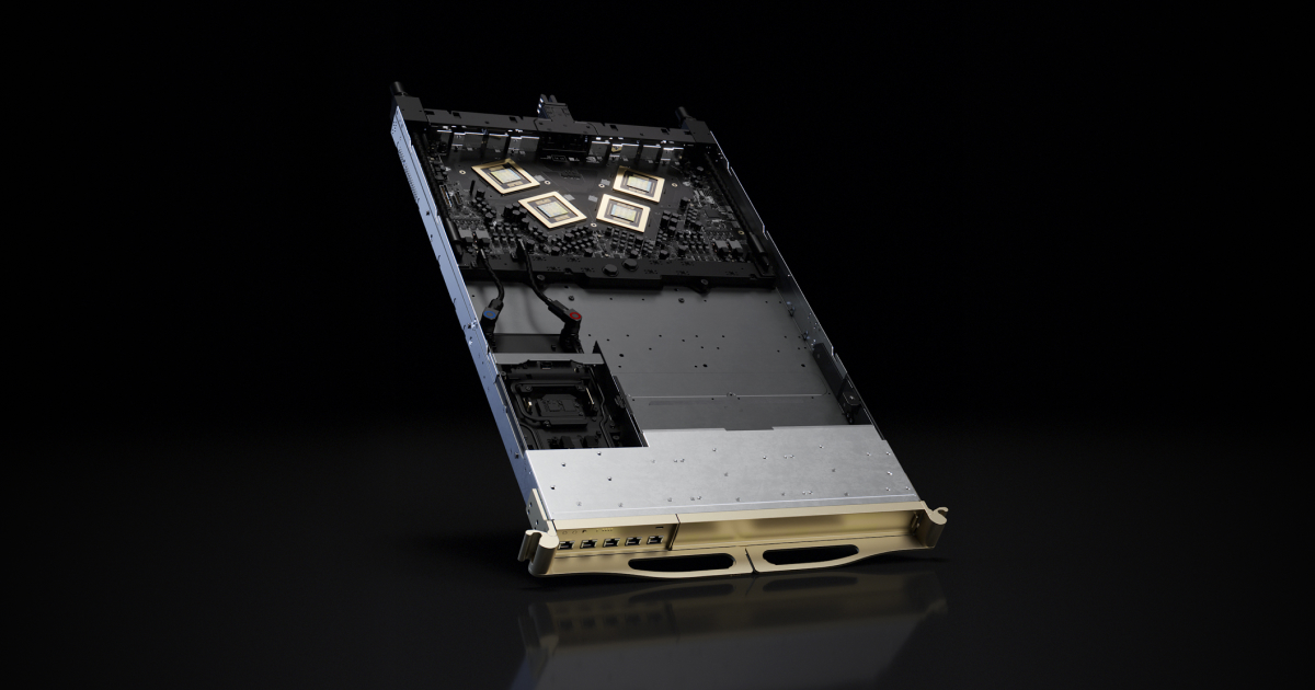
The NVIDIA® Grace Hopper architecture brings together the groundbreaking performance of the NVIDIA Hopper GPU with the versatility of the NVIDIA Grace™ CPU, connected with a high bandwidth and memory coherent NVIDIA NVLink Chip-2-Chip (C2C)® interconnect in a single Superchip, and support for...
resources.nvidia.com
Notice that in the diagram on page 7, Nvidia refers to the two implementations of NVLinks separately.
Of course, Nvidia has never published a deep-dive on NVLink that I've seen, so I could still be wrong. If you've seen documents that contradict my conclusions, I've love to read them.
Yah but the modes 1 and 2 for IO and for Coherence/Cache are tall messy stacks and mode 1 is essentially a repeat of the PCIe stack. Anyway, I think we both agree PCIe is trailing edge compatibility. CXL had some good ideas, but AI (properly) moved the goalposts to another county.
Back to the original topic of software for AI - just watched all four of the Computex keynotes, from NVIDIA, AMD, Qualcomm and Intel. NVIDIA offered the only keynote that focused in specifically on tools for creation, training, deployment, scale-up, and scale-out of Gen AI applications. The rest essentially punted to "the ecosystem" which really only consisted of Microsoft (the same "phoned-in" performance from Satya at each), except for AMD which also included trivial apps from Lenovo and emerging apps from Stability.ai. OK, maybe Intel was showing a demo-ware app with their open source RAG stuff, but that's just a bunch of open source pieces grafted together, not a production app.
GPU-to-GPU I/O exists on NVLinks, and NVLink appears to use a form of RDMA to allow GPUs to access each other's memories at the physical address level, but I've seen no evidence there is cache coherency on standard NVLinks.
NVlink is used to bind your cluster together. In low level code for NV GPUs you can read and write memory anywhere in cluster global memory. Nvidia do discuss coherent memory access. This is load/store over NVlink, not RDMA unless the route has to tunnel through IB, which in the H100 is not being used between the local 8 GPUs.
It occurred to me while I laying in a hotel bed in San Diego a couple of nights ago that there is indeed a version of NVLink, called NVLink-C2C, which is used for inter-processor cache coherency in Grace Hooper, and that was perhaps what you were thinking about.
That is just NVLink with a more efficient short range Phy. They have an ultra-short one in Blackwell between the two dies in one package, and the short one between Blackwell packages, which are both called NVLink and both clearly fabric extensions, and neither the same as the 50cm one that Blackwell uses to reach the switches on other shelves. But all of those are fabric extensions.
The links in CXL are PCIe. The protocols for CXL are not exactly PCIe, even in mode 1. But they are still clogged with latency and backwards compatibility and various features to support class IO model.