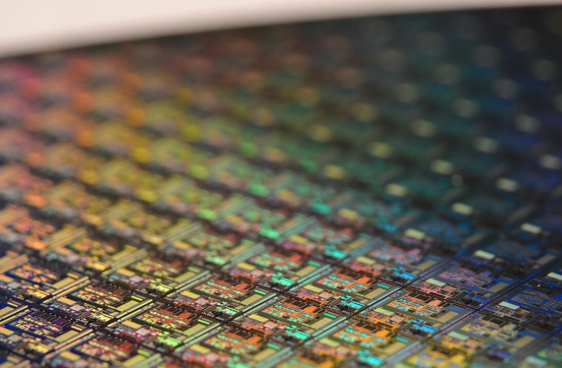
A domestic lithographic complex consisting of installations for maskless image acquisition on a substrate and plasma-chemical etching of silicon has been created in St. Petersburg. The developers claim that the first machine used for maskless nanolithography costs around 5 million rubles, that is, the same as a modern Chinese car of good quality, while foreign analogues are valued at billions of rubles.
Nanobreakthrough of Russia
Specialists from Peter the Great St. Petersburg Polytechnic University ( SPbPU ) have developed two installations for the production of microelectronic nanostructures, which will make it possible to “resolve the issue of Russia’s technological sovereignty in this direction in the field of microelectronics ,” RIA Novosti writes, citing representatives of the university. The complex of devices includes installations for maskless nanolithography and plasma-chemical etching of silicon .
The first installation is used to obtain an image on the substrate, without using a special mask. This technology, according to the developers, is much less expensive compared to classical lithography, both in terms of money and time, in which specialized templates are used to obtain images. The installation is controlled by specialized software and is fully automated.
According to the agency, such an installation is estimated at approximately 5 million rubles, that is, it is comparable in price to many modern Chinese cars, for example, the Geely Monjaro crossover. RIA also provides a comparison with foreign installations of this type - the agency claims that it costs tens of times more, in the range of 10-13 billion rubles.
Development number two
The complex, developed at St. Petersburg Polytechnic University, is designed to create nanostructures necessary “for the operation of various microelectronic equipment,” university representatives told the agency. A base-mask lithograph is used in the first stage of this process, then a machine for plasma chemical etching of silicon is useful in the second.

Photo: Laura Ockel / Unsplash
Russian lithography has become a little more modern
The second installation uses the pattern on the substrate created in the first stage. It is intended directly for the formation of nanostructures, but also allows the creation of silicon membranes, which can later be used, for example, in ship gauge pressure sensors, RIA Novosti writes.
The authors of the project assured the agency that the membranes created using such a facility “are superior in reliability and sensitivity to those produced by liquid or laser etching.” They also emphasized that this is a completely domestic product.
Its creators did not disclose the cost of the second installation.
Potential range of applications and future plans
A complex of two installations, created in the bowels of St. Petersburg Polytechnic University , can be used, among other things, to increase the service life of radar equipment by more than 20 times, Artem Osipov, head of the laboratory “Technology of Materials and Electronic Products” of St. Petersburg Polytechnic University, told the agency . He also added that if installations are used in the production of solar panels, it will be possible to reduce their weight and size and teach them to work in cloudy weather with the same high efficiency as in bright sun .
The developers do not specify whether any of the Russian chip manufacturers are interested in their new installations. In this regard, there is no information when they will begin to be used in real production. Meanwhile, the inventors continue to improve the lithography complex they created. In particular, they intend to equip both installations included in it with artificial intelligence , without specifying exactly what tasks it will solve.
Competitors are not asleep
SPbPU is not the only university striving to create advanced domestic solutions for lithography. Back in October 2022, CNews wrote that the Nizhny Novgorod Institute of Applied Physics of the Russian Academy of Sciences ( IPF RAS ) had begun work in this direction , but its goal was slightly different.
As is known, as of October 2023, Russia was not able to produce microcircuits using modern technological processes - the country has access to a maximum of 65- nanometer topology, which was outdated almost 20 years ago. Now a 28-nanometer factory is being built, but this technical process has long lost its relevance - the 4 nm technical process has long been mastered, and in 2023 the transition to 3 nm took place.
IAP RAS is striving to reduce such a striking gap between Russia and the rest of the world - university specialists are developing the first domestic lithograph that will be able to produce chips using a 7 nm topology. However, this will take them years – the equipment may not begin full-fledged operation until 2028.
Also in March 2023, CNews wrote that the Ministry of Industry and Trade ordered the development and development of production of lithographic materials for microelectronic production, in particular, photoresists. The ministry will pay 1.1 billion rubles for this work.

Nanobreakthrough of Russia
Specialists from Peter the Great St. Petersburg Polytechnic University ( SPbPU ) have developed two installations for the production of microelectronic nanostructures, which will make it possible to “resolve the issue of Russia’s technological sovereignty in this direction in the field of microelectronics ,” RIA Novosti writes, citing representatives of the university. The complex of devices includes installations for maskless nanolithography and plasma-chemical etching of silicon .
The first installation is used to obtain an image on the substrate, without using a special mask. This technology, according to the developers, is much less expensive compared to classical lithography, both in terms of money and time, in which specialized templates are used to obtain images. The installation is controlled by specialized software and is fully automated.
According to the agency, such an installation is estimated at approximately 5 million rubles, that is, it is comparable in price to many modern Chinese cars, for example, the Geely Monjaro crossover. RIA also provides a comparison with foreign installations of this type - the agency claims that it costs tens of times more, in the range of 10-13 billion rubles.
Development number two
The complex, developed at St. Petersburg Polytechnic University, is designed to create nanostructures necessary “for the operation of various microelectronic equipment,” university representatives told the agency. A base-mask lithograph is used in the first stage of this process, then a machine for plasma chemical etching of silicon is useful in the second.

Photo: Laura Ockel / Unsplash
Russian lithography has become a little more modern
The second installation uses the pattern on the substrate created in the first stage. It is intended directly for the formation of nanostructures, but also allows the creation of silicon membranes, which can later be used, for example, in ship gauge pressure sensors, RIA Novosti writes.
The authors of the project assured the agency that the membranes created using such a facility “are superior in reliability and sensitivity to those produced by liquid or laser etching.” They also emphasized that this is a completely domestic product.
Its creators did not disclose the cost of the second installation.
Potential range of applications and future plans
A complex of two installations, created in the bowels of St. Petersburg Polytechnic University , can be used, among other things, to increase the service life of radar equipment by more than 20 times, Artem Osipov, head of the laboratory “Technology of Materials and Electronic Products” of St. Petersburg Polytechnic University, told the agency . He also added that if installations are used in the production of solar panels, it will be possible to reduce their weight and size and teach them to work in cloudy weather with the same high efficiency as in bright sun .
The developers do not specify whether any of the Russian chip manufacturers are interested in their new installations. In this regard, there is no information when they will begin to be used in real production. Meanwhile, the inventors continue to improve the lithography complex they created. In particular, they intend to equip both installations included in it with artificial intelligence , without specifying exactly what tasks it will solve.
Competitors are not asleep
SPbPU is not the only university striving to create advanced domestic solutions for lithography. Back in October 2022, CNews wrote that the Nizhny Novgorod Institute of Applied Physics of the Russian Academy of Sciences ( IPF RAS ) had begun work in this direction , but its goal was slightly different.
As is known, as of October 2023, Russia was not able to produce microcircuits using modern technological processes - the country has access to a maximum of 65- nanometer topology, which was outdated almost 20 years ago. Now a 28-nanometer factory is being built, but this technical process has long lost its relevance - the 4 nm technical process has long been mastered, and in 2023 the transition to 3 nm took place.
IAP RAS is striving to reduce such a striking gap between Russia and the rest of the world - university specialists are developing the first domestic lithograph that will be able to produce chips using a 7 nm topology. However, this will take them years – the equipment may not begin full-fledged operation until 2028.
Also in March 2023, CNews wrote that the Ministry of Industry and Trade ordered the development and development of production of lithographic materials for microelectronic production, in particular, photoresists. The ministry will pay 1.1 billion rubles for this work.

В России создан суверенный литограф для выпуска микросхем. Он стоит как китайский автомобиль - CNews
В Санкт-Петербурге создан отечественный литографический комплекс из установок для безмасочного получения изображения...
www.cnews.ru
