IBM’s NorthPole processor sidesteps need to access external memory, boosting computing power and saving energy.
.")
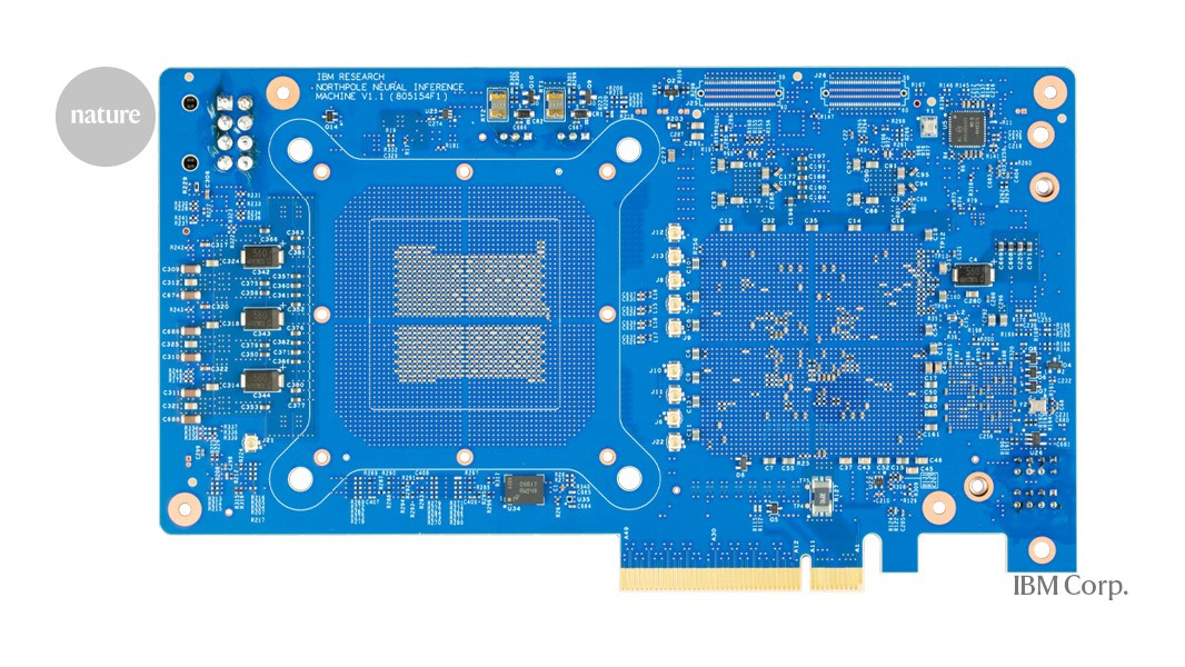
The NorthPole chip developed by IBM brings memory and processing together, allowing vast improvements in image recognition and other computing tasksCredit: IBM Corp.
A brain-inspired computer chip that could supercharge artificial intelligence (AI) by working faster with much less power has been developed by researchers at IBM in San Jose, California. Their massive NorthPole processor chip eliminates the need to frequently access external memory, and so performs tasks such as image recognition faster than existing architectures do — while consuming vastly less power.
“Its energy efficiency is just mind-blowing,” says Damien Querlioz, a nanoelectronics researcher at the University of Paris-Saclay in Palaiseau. The work, published in Science1, shows that computing and memory can be integrated on a large scale, he says. “I feel the paper will shake the common thinking in computer architecture.”
NorthPole runs neural networks: multi-layered arrays of simple computational units programmed to recognize patterns in data. A bottom layer takes in data, such as the pixels in an image; each successive layer detects patterns of increasing complexity and passes information on to the next layer. The top layer produces an output that, for example, can express how likely an image is to contain a cat, a car or other objects.
The Von Neumann bottleneck is one of the most significant factors that slow computer applications — including AI. It also results in energy inefficiencies. Study co-author Dharmendra Modha, a computer engineer at IBM, says he once estimated that simulating a human brain on this type of architecture might require the equivalent of the output of 12 nuclear reactors.
NorthPole is made of 256 computing units, or cores, each of which contains its own memory. “You’re mitigating the Von Neumann bottleneck within a core,” says Modha, who is IBM’s chief scientist for brain-inspired computing at the company’s Almaden research centre in San Jose.
The cores are wired together in a network inspired by the white-matter connections between parts of the human cerebral cortex, Modha says. This and other design principles — most of which existed before but had never been combined in one chip — enable NorthPole to beat existing AI machines by a substantial margin in standard benchmark tests of image recognition. It also uses one-fifth of the energy of state-of-the-art AI chips, despite not using the most recent and most miniaturized manufacturing processes. If the NorthPole design were implemented with the most up-to-date manufacturing process, its efficiency would be 25 times better than that of current designs, the authors estimate.
NorthPole brings memory units as physically close as possible to the computing elements in the core. Elsewhere, researchers have been developing more-radical innovations using new materials and manufacturing processes. These enable the memory units themselves to perform calculations, which in principle could boost both speed and efficiency even further.
Another chip, described last month2, does in-memory calculations using memristors, circuit elements able to switch between being a resistor and a conductor. “Both approaches, IBM’s and ours, hold promise in mitigating latency and reducing the energy costs associated with data transfers,” says Bin Gao at Tsinghua University, Beijing, who co-authored the memristor study.
Another approach, developed by several teams — including one at a separate IBM lab in Zurich, Switzerland3 — stores information by changing a circuit element’s crystal structure. It remains to be seen whether these newer approaches can be scaled up economically.
doi: https://doi.org/10.1038/d41586-023-03267-0
 www.nature.com
- NEWS
- 19 October 2023
‘Mind-blowing’ IBM chip speeds up AI
IBM’s NorthPole processor sidesteps need to access external memory, boosting computing power and saving energy.
The NorthPole chip developed by IBM brings memory and processing together, allowing vast improvements in image recognition and other computing tasksCredit: IBM Corp.
A brain-inspired computer chip that could supercharge artificial intelligence (AI) by working faster with much less power has been developed by researchers at IBM in San Jose, California. Their massive NorthPole processor chip eliminates the need to frequently access external memory, and so performs tasks such as image recognition faster than existing architectures do — while consuming vastly less power.
“Its energy efficiency is just mind-blowing,” says Damien Querlioz, a nanoelectronics researcher at the University of Paris-Saclay in Palaiseau. The work, published in Science1, shows that computing and memory can be integrated on a large scale, he says. “I feel the paper will shake the common thinking in computer architecture.”
NorthPole runs neural networks: multi-layered arrays of simple computational units programmed to recognize patterns in data. A bottom layer takes in data, such as the pixels in an image; each successive layer detects patterns of increasing complexity and passes information on to the next layer. The top layer produces an output that, for example, can express how likely an image is to contain a cat, a car or other objects.
Slowed by a bottleneck
Some computer chips can handle these calculations efficiently, but they still need to use external memory called RAM each time they calculate a layer. Shuttling data between chips in this way slows things down — a phenomenon known as the Von Neumann bottleneck, after mathematician John von Neumann, who first conceived the standard architecture of computers based on a processing unit and a separate memory unit.The Von Neumann bottleneck is one of the most significant factors that slow computer applications — including AI. It also results in energy inefficiencies. Study co-author Dharmendra Modha, a computer engineer at IBM, says he once estimated that simulating a human brain on this type of architecture might require the equivalent of the output of 12 nuclear reactors.
NorthPole is made of 256 computing units, or cores, each of which contains its own memory. “You’re mitigating the Von Neumann bottleneck within a core,” says Modha, who is IBM’s chief scientist for brain-inspired computing at the company’s Almaden research centre in San Jose.
The cores are wired together in a network inspired by the white-matter connections between parts of the human cerebral cortex, Modha says. This and other design principles — most of which existed before but had never been combined in one chip — enable NorthPole to beat existing AI machines by a substantial margin in standard benchmark tests of image recognition. It also uses one-fifth of the energy of state-of-the-art AI chips, despite not using the most recent and most miniaturized manufacturing processes. If the NorthPole design were implemented with the most up-to-date manufacturing process, its efficiency would be 25 times better than that of current designs, the authors estimate.
On the right road
But even NorthPole’s 224 megabytes of RAM are not enough for large language models, such as those used by the chatbot ChatGPT, which take up several thousand megabytes of data even in their most stripped-down versions. And the chip can run only pre-programmed neural networks that need to be ‘trained’ in advance on a separate machine. But the paper’s authors say that the NorthPole architecture could be useful in speed-critical applications, such as self-driving cars.NorthPole brings memory units as physically close as possible to the computing elements in the core. Elsewhere, researchers have been developing more-radical innovations using new materials and manufacturing processes. These enable the memory units themselves to perform calculations, which in principle could boost both speed and efficiency even further.
Another chip, described last month2, does in-memory calculations using memristors, circuit elements able to switch between being a resistor and a conductor. “Both approaches, IBM’s and ours, hold promise in mitigating latency and reducing the energy costs associated with data transfers,” says Bin Gao at Tsinghua University, Beijing, who co-authored the memristor study.
Another approach, developed by several teams — including one at a separate IBM lab in Zurich, Switzerland3 — stores information by changing a circuit element’s crystal structure. It remains to be seen whether these newer approaches can be scaled up economically.
doi: https://doi.org/10.1038/d41586-023-03267-0
‘Mind-blowing’ IBM chip speeds up AI
IBM’s NorthPole processor sidesteps need to access external memory, boosting computing power and saving energy.
www.nature.com