Array
(
    [content] => 
    [params] => Array
        (
            [0] => /forum/index.php?threads/it%E2%80%99s-official-high-na-euv-will-get-a-successor.20243/
        )

    [addOns] => Array
        (
            [DL6/MLTP] => 13
            [Hampel/TimeZoneDebug] => 1000070
            [SV/ChangePostDate] => 2010200
            [SemiWiki/Newsletter] => 1000010
            [SemiWiki/WPMenu] => 1000010
            [SemiWiki/XPressExtend] => 1000010
            [ThemeHouse/XLink] => 1000970
            [ThemeHouse/XPress] => 1010570
            [XF] => 2021370
            [XFI] => 1050270
        )

    [wordpress] => /var/www/html
)

It’s official: High-NA EUV will get a successor

Daniel Nenni

Admin
Staff member
"In ten years from now, we’ll have a single platform of low-NA, high-NA and hyper-NA,” according to Martin van den Brink at Imec’s Technology Forum.

ASML is proceeding with the development of a hyper-NA EUV tool. “In ten years from now, we’ll have a single platform of low-NA, high-NA and hyper-NA EUV systems,” emeritus CTO Martin van den Brink said in a presentation at Imec’s Technology Forum (ITF) in Antwerp today. He argued that the availability of such an even higher resolution tool is crucial to reducing the number of process steps, thereby cutting the cost and energy needed to process a wafer. “Hyper-NA allows us to stay away from the dangerous complexity of double patterning,” Van den Brink said.

20240521 Imec ITF RR201264


The announcement arrives at a time when high-NA EUV lithography has barely got going. ASML started shipping high-NA tools last December and will in a matter of weeks officially open the High-NA Lab in Veldhoven, a facility co-run with Imec providing chipmakers with early access to the tool. The system in that lab is already operational, however, and as announced in a post on X last month, it printed the first-ever 10nm line pattern. Van den Brink had an update about that too: an 8nm line pattern was produced, which is near the maximum resolution of the tool.
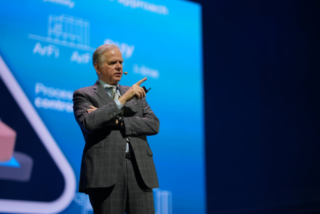
 
"In ten years from now, we’ll have a single platform of low-NA, high-NA and hyper-NA,” according to Martin van den Brink at Imec’s Technology Forum.

ASML is proceeding with the development of a hyper-NA EUV tool. “In ten years from now, we’ll have a single platform of low-NA, high-NA and hyper-NA EUV systems,” emeritus CTO Martin van den Brink said in a presentation at Imec’s Technology Forum (ITF) in Antwerp today. He argued that the availability of such an even higher resolution tool is crucial to reducing the number of process steps, thereby cutting the cost and energy needed to process a wafer. “Hyper-NA allows us to stay away from the dangerous complexity of double patterning,” Van den Brink said.

20240521 Imec ITF RR201264


The announcement arrives at a time when high-NA EUV lithography has barely got going. ASML started shipping high-NA tools last December and will in a matter of weeks officially open the High-NA Lab in Veldhoven, a facility co-run with Imec providing chipmakers with early access to the tool. The system in that lab is already operational, however, and as announced in a post on X last month, it printed the first-ever 10nm line pattern. Van den Brink had an update about that too: an 8nm line pattern was produced, which is near the maximum resolution of the tool.


ASML CTO Van den Brink used to believe that hyper-NA is not viable during @pgerven interview with him in 2022. What has changed since 2022 that he started thinking Hyper NA EUV is a feasible future?

"This phenomenon also plays out with an increase in lens aperture (numerical aperture, NA). So is another increase in NA a possibility? ASML is looking into it, Van den Brink confirms. But, personally, he doesn’t believe that hyper-NA will prove viable. “We’re researching it, but that doesn’t mean it will make it into production. For years, I’ve been suspecting that high-NA will be the last NA, and this belief hasn’t changed.”"

Source: https://semiwiki.com/forum/index.php?threads/high-na-might-be-last-gen-litho.16753/
 
Will user accept to pay several millions more $ to scale ~2-5nm when scaling becomes slow down and chip/transistor cost per area are increasing? It will be very hard to justify.
 
Will user accept to pay several millions more $ to scale ~2-5nm when scaling becomes slow down and chip/transistor cost per area are increasing? It will be very hard to justify.
Could this cause chip designs to move towards hyper-specialization / accelerator-type stuff to keep up performance per-mm improvements?
 
Could this cause chip designs to move towards hyper-specialization / accelerator-type stuff to keep up performance per-mm improvements?
This is already happening, because application-dedicated hardware is much more performant than general purpose CPUs, can simultaneously have lower power consumption for the similar or better performance, and manufacturing costs can be much less because die areas are smaller and often don't require chiplets. The problem is that hyper-specialized designs, as you put it, typically have lower unit volumes than general purpose designs, so the R&D per unit can be effectively higher, and the production volume lower, which means stuff like mask sets, analog design, etc., don't get divided down by the larger production numbers that general purpose chips typically have.
 
Last edited:
ASML CTO Van den Brink used to believe that hyper-NA is not viable during @pgerven interview with him in 2022. What has changed since 2022 that he started thinking Hyper NA EUV is a feasible future?

"This phenomenon also plays out with an increase in lens aperture (numerical aperture, NA). So is another increase in NA a possibility? ASML is looking into it, Van den Brink confirms. But, personally, he doesn’t believe that hyper-NA will prove viable. “We’re researching it, but that doesn’t mean it will make it into production. For years, I’ve been suspecting that high-NA will be the last NA, and this belief hasn’t changed.”"

Source: https://semiwiki.com/forum/index.php?threads/high-na-might-be-last-gen-litho.16753/
From that same interview:
The main goal of the hyper-NA research program is therefore to come up with smart solutions that keep the technology manageable in terms of cost and manufacturability. Van den Brink doesn’t want to have to build even larger monsters, he says, gesturing to a miniature version of the metrology vessel in his collection, but also referring to scanner components such as the lenses. “We’re trying to come up with fundamental changes in manufacturing and design to make sure that if we’re going to do it, it will be economically feasible.”

As time advances technology improves. Remember when folks said there was no economic way to continue scaling because of the end of Dennard scaling, because 248nm hit the resolution limit, or not having EUV by 45nm would doom us since 193nm dry hit it's limit at 65nm nodes. The chip makers and tool vendors make the impossible possible.

Also having lead customers helps:
"In April 2023, Van den Brink’s confidence in the hyper-NA business case had grown even more. “I’ve traveled several times around the world talking to customers about the need and desirability of hyper-NA. In recent months, I’ve gained the confidence and insight that customers want to drive the resolution down so much further that the opportunity for using hyper-NA for mass production of logic and memory chips is there,” he told Dutch tech website Tweakers (link in Dutch)."
If there is demand from chip makers than ASML will find a way to make it happen (although let's hope "the way" is faster than the 30 or so years that low-NA EUV needed ;))
 
"In ten years from now, we’ll have a single platform of low-NA, high-NA and hyper-NA,” according to Martin van den Brink at Imec’s Technology Forum.

ASML is proceeding with the development of a hyper-NA EUV tool. “In ten years from now, we’ll have a single platform of low-NA, high-NA and hyper-NA EUV systems,” emeritus CTO Martin van den Brink said in a presentation at Imec’s Technology Forum (ITF) in Antwerp today. He argued that the availability of such an even higher resolution tool is crucial to reducing the number of process steps, thereby cutting the cost and energy needed to process a wafer. “Hyper-NA allows us to stay away from the dangerous complexity of double patterning,” Van den Brink said.

20240521 Imec ITF RR201264


The announcement arrives at a time when high-NA EUV lithography has barely got going. ASML started shipping high-NA tools last December and will in a matter of weeks officially open the High-NA Lab in Veldhoven, a facility co-run with Imec providing chipmakers with early access to the tool. The system in that lab is already operational, however, and as announced in a post on X last month, it printed the first-ever 10nm line pattern. Van den Brink had an update about that too: an 8nm line pattern was produced, which is near the maximum resolution of the tool.

The hyper-NA depth of focus is 10 nm, that is too thin for any resist to support an exposure.
 
ASML trying to stay relevant despite electrons in resists.

TSMC publicly said they don't need High NA EUV in the near future and High NA is too expensive to be considered at this point.

But if we can learn something from the 300mm to 450mm wafer migration history, it's possible that there are additional and important reasons behind such decisions. Except TSMC can't reveal them right now.


Too expensive?Interesting, I thought a monopoly like TSMC can charge whatever they want

It is easy to knock price but the reality is HNA EUV is not ready for Apple SoC HVM and that is always first for TSMC. Apple is TSMC's biggest supporter and they are not doing chiplets so TSMC must HVM Ax SoCs right out of the gate. And just as Hauwei will get to 5nm without EUV, TSMC certainly can develop sub 2nm without HNA EUV.

I have spent 40 years in the semiconductor industry and have seen many mind blowing innovations that supposedly could not be done. This industry is full of very intelligent people and the money to be made is staggering. Do not bet against TSMC, absolutely.
 
TSMC publicly said they don't need High NA EUV in the near future and High NA is too expensive to be considered at this point.

But if we can learn something from the 300mm to 450mm wafer migration history, it's possible that there are additional and important reasons behind such decisions. Except TSMC can't reveal them right now.


TSMC didn’t say that. Read their earnings statement. They said it wasn’t necessary for 2nm but adopting high-NA would allow for a cheaper flow. Reading between the lines the “issue” seems to just be as simple as N2/A16 BEOLs (since all indication is that these layers are mostly unchanged from N3 to ease development) are ready before even intel wants to use high-NA and TSMC would need more scanners than intel would.
 
TSMC didn’t say that. Read their earnings statement. They said it wasn’t necessary for 2nm but adopting high-NA would allow for a cheaper flow. Reading between the lines the “issue” seems to just be as simple as N2/A16 BEOLs (since all indication is that these layers are mostly unchanged from N3 to ease development) are ready before even intel wants to use high-NA and TSMC would need more scanners than intel would.

I think he was referencing what was said at the TSMC Symposium versus what was said on the earnings call. Kevin Zhang said it in the press briefing.

Cost is easy to call out but HNA EUV not working yet is a less popular comment or the inability to get enough systems in time for A16 HVM.
 
TSMC didn’t say that. Read their earnings statement. They said it wasn’t necessary for 2nm but adopting high-NA would allow for a cheaper flow. Reading between the lines the “issue” seems to just be as simple as N2/A16 BEOLs (since all indication is that these layers are mostly unchanged from N3 to ease development) are ready before even intel wants to use high-NA and TSMC would need more scanners than intel would.

Here is what TSMC said about adopting High NA EUV:

"Zhang said that TSMC does not believe it needs to use a ASML's (ASML.AS), new "High NA EUV" lithography tool machines to build the A16 chips. Intel last week revealed that it plans to be the first to use the machines, which can cost $373 million each, to develop its 14A chip."


""I like the technology but I don't like the sticker price", Zhang told reporters. TSMC's A16 node will follow its 2 nanometer production node, which is expected to enter mass production in 2025."

 
Last edited:
Cost is easy to call out but HNA EUV not working yet is a less popular comment or the inability to get enough systems in time for A16 HVM.
This was my totally non-expert guess. They couldn't get enough HNA machines in time anyway, TSMC doesn't need to prove anything with a flashy intro the way Intel did, so TSMC is working out how to make do for A16 with their EUV machines. What else could they do except delay?
 
I really hope in 5-10 years we’ll be able to read how TSMC made it’s decisions around this time (N2, A16, BSPD, adv packaging changes), and what Intel looked like internally (engineering view) for 5N4Y and the first generation of High NA - 14A.

I’d like to hear about what kind of backup plans TSMC and Intel have in place right now, how TSMC chose it’s density targets for N2 and A16, and hear (definitively) about how much Intel’s High NA decision is based on marketing vs. engineering.

This seems like a pretty big inflection point in chip fabrication.

I feel the same way. TSMC does not need to take big technology risks since they are the market leader by a large margin. Intel must take risks to catch TSMC. I think both companies are making the correct decisions. We will know in 5 years.
 
I think he was referencing what was said at the TSMC Symposium versus what was said on the earnings call. Kevin Zhang said it in the press briefing.

Cost is easy to call out but HNA EUV not working yet is a less popular comment or the inability to get enough systems in time for A16 HVM.
Since A16 is just N2+BSPD I think a more accurate statement is that they couldn't get it in time for N2 HVM, because I have a hard time imagining that any cost benefit high-NA might eventually offer would be so great to warrant deinstalling low-NA tools that haven't even paid for themselves yet and reinstalling new high-NA tools in Fab 20 (assuming F20 can even support high-NA tools which I wouldn't assume since TSMC would have known well ahead of time that high-NA wouldn't be ready in 2024 when they started F20 fit up).
 
Back
Top