Array
(
    [content] =>
    [params] => Array
        (
            [0] => /forum/threads/it%E2%80%99s-official-high-na-euv-will-get-a-successor.20243/page-2
        )

    [addOns] => Array
        (
            [DL6/MLTP] => 13
            [Hampel/TimeZoneDebug] => 1000070
            [SV/ChangePostDate] => 2010200
            [SemiWiki/Newsletter] => 1000010
            [SemiWiki/WPMenu] => 1000010
            [SemiWiki/XPressExtend] => 1000010
            [ThemeHouse/XLink] => 1000970
            [ThemeHouse/XPress] => 1010570
            [XF] => 2031070
            [XFI] => 1060170
        )

    [wordpress] => /var/www/html
)
Guests have limited access.
Join our community today!
Join our community today!
You are currently viewing SemiWiki as a guest which gives you limited access to the site. To view blog comments and experience other SemiWiki features you must be a registered member. Registration is fast, simple, and absolutely free so please, join our community today!
You are using an out of date browser. It may not display this or other websites correctly.
You should upgrade or use an alternative browser.
You should upgrade or use an alternative browser.
It’s official: High-NA EUV will get a successor
- Thread starter Daniel Nenni
- Start date
If we retrospect and learn from history, when will we think Hi NA EUV be ready for HVM? 2026? Before 2030?
View attachment 1938
Full EUV was 2020 with TSMC N5 but I guess you could claim N7+ in 2019.
When will Intel have HNA-EUV chiplets? TSMC needs to do full chip so my guess is 2028.
hist78
Well-known member
If we retrospect and learn from history, when will we think Hi NA EUV be ready for HVM? 2026? Before 2030?
View attachment 1938
Or, 2036 for the High NA EUV HVM, using the 12 years difference between IMEC R&D and industry adoption from the EUV deployment history.
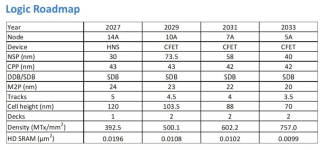
And N2 is pretty much N3 with HNS transistors replacing FinFETs, the basic pitches (metal and contacted poly) hardly changed. That's three headline process generations (N3/N2/A16) with almost identical underlying technology...Since A16 is just N2+BSPD I think a more accurate statement is that they couldn't get it in time for N2 HVM, because I have a hard time imagining that any cost benefit high-NA might eventually offer would be so great to warrant deinstalling low-NA tools that haven't even paid for themselves yet and reinstalling new high-NA tools in Fab 20 (assuming F20 can even support high-NA tools which I wouldn't assume since TSMC would have known well ahead of time that high-NA wouldn't be ready in 2024 when they started F20 fit up).
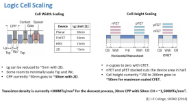
If you want another example of how marketing has taken over the process circus, look at actual physical gate length instead on the headline "Xnm" number -- this has been static at around 16nm for many Finfet generations all the way down to the last one (N3), in spite of what is drawn or labelled. Even switching to HNS for N2/A16 and similar (and future HNS processes) this only drops to about 13nm, and CPP and MP have pretty much stalled...
Attachments
That is the key observation. Channel control is limited by end effects which bottom out at 16nm for fins, 13nm for ribbons, using Si. There are indications that W/Mo S2 2-D materials could go down to 10nm with adequate control but those are not even on roadmap, and who knows if they will solve the problem of building source/drain contacts in a compact way.If you want another example of how marketing has taken over the process circus, look at actual physical gate length instead on the headline "Xnm" number -- this has been static at around 16nm for many Finfet generations all the way down to the last one (N3), in spite of what is drawn or labelled. Even switching to HNS for N2/A16 and similar (and future HNS processes) this only drops to about 13nm, and CPP and MP have pretty much stalled...
The 13nm ribbon length comes with a 4th side so capacitance/nm goes up, meaning the CV^2/2 switching energy is not moving. Increased perfection in materials may deliver some Ceff reduction, but overall we have been near perfection for a silicon channel for a while.
Functions like matmul which dominate AI will reach power densities that cannot be cooled if they shrink without solving C and V.
Right. And please look at the date of J.P. publication by IanD. I remember seeing his presentation at IEDM 1990 where GAA was already there and some of his early 2000s papers on advantages and disadvantages of various device structures. Unfortunately marketing took over 
Issues with 2D materials will require a lot of work before they can be introduced. Even assuming a good fabrication method for them is found, the physical issues of making low resistance contacts between a 2D semiconductor and a 3D metal or semiconductor is always there let alone its size. It can easily be the limiting factor compared to CV^2/2. Plus its topology will not be much different than HNS or CFET variants so same issues in litho. No magic bullets.
Issues with 2D materials will require a lot of work before they can be introduced. Even assuming a good fabrication method for them is found, the physical issues of making low resistance contacts between a 2D semiconductor and a 3D metal or semiconductor is always there let alone its size. It can easily be the limiting factor compared to CV^2/2. Plus its topology will not be much different than HNS or CFET variants so same issues in litho. No magic bullets.
My bet is on going cold, with device materials engineered for low voltage thresholds. I don't see it shrinking devices but it will allow more work done with less power:No magic bullets.

From that same interview:
As time advances technology improves. Remember when folks said there was no economic way to continue scaling because of the end of Dennard scaling, because 248nm hit the resolution limit, or not having EUV by 45nm would doom us since 193nm dry hit it's limit at 65nm nodes. The chip makers and tool vendors make the impossible possible.
Also having lead customers helps:
If there is demand from chip makers than ASML will find a way to make it happen (although let's hope "the way" is faster than the 30 or so years that low-NA EUV needed)
This would be my take as well. I'm planning an article detailing how far ASML believes it can take dimensional scaling cost-effectively.
I should note that I initially worded the title of the article quoted in the opening post too strongly, and it has been updated accordingly. I don't think ASML/Van den Brink would be talking publicly about hyper-NA if development wasn't far along, though. My guess is they're dotting the i's.
I suspect they anticipate High-NA performance won't be so great, need a next step. The interception is close to original projected HVM of High-NA.This would be my take as well. I'm planning an article detailing how far ASML believes it can take dimensional scaling cost-effectively.
I should note that I initially worded the title of the article quoted in the opening post too strongly, and it has been updated accordingly. I don't think ASML/Van den Brink would be talking publicly about hyper-NA if development wasn't far along, though. My guess is they're dotting the i's.
Will you discuss electrons in your article?
I suspect they anticipate High-NA performance won't be so great, need a next step. The interception is close to original projected HVM of High-NA.
Will you discuss electrons in your article?
That sounds more like an Imec thing. But isn't it always the case that certain requirements seem unattainable early on, only to be met eventually anyhow?
No. It will be an enormous effort that cannot be hidden, which is why they need to talk about it. Shareholders must be aware.I don't think ASML/Van den Brink would be talking publicly about hyper-NA if development wasn't far along, though. My guess is they're dotting the i's.
Dotting the i's is where High NA hopes it is now. Like MOx resists thought they were 2 years ago... and they are still dotting them.
Except for the additional power (and space and cost and complexity) needed to keep things cold, which in reality is likely to be bigger than the chip power saved by running cold especially for small systems/solutions...My bet is on going cold, with device materials engineered for low voltage thresholds. I don't see it shrinking devices but it will allow more work done with less power:

(yes I read the paper you linked to, and it kind of ignores the realities of what is needed to run stuff at LN2 temperatures in the real world as opposed to the lab -- not just efficiency but cost/size which doesn't scale down)
Here is what TSMC said about adopting High NA EUV:
"Zhang said that TSMC does not believe it needs to use a ASML's (ASML.AS), new "High NA EUV" lithography tool machines to build the A16 chips. Intel last week revealed that it plans to be the first to use the machines, which can cost $373 million each, to develop its 14A chip."
""I like the technology but I don't like the sticker price", Zhang told reporters. TSMC's A16 node will follow its 2 nanometer production node, which is expected to enter mass production in 2025."
TSMC did not say that, Kevin did, and he was in hot water for it.
I was there, he said it in a press lunch not during his Symposium presentation. It was off the cuff, not scripted, we were peppering him with HNA-EUV questions. His not liking the sticker price comment was his personal opinion. I have not heard anyone else at TSMC say that. They would also not say officially that HNA-EUV does not work or has technical issues which it most certainly does. TSMC does not want to piss off ASML.
Seeing it in person and reading it is two different things. Tone, body language, context matters.
Oh I'm not saying it does not pose difficulties. It will take a while. But LN2 chilling is already scaled, so the main problems are in the silicon and the modularity for maintenance. Networking will be interesting since glass gets brittle. I expect reliability to be quite high, as has been the pattern for improved cooling in servers at less extreme temps. The main factors appear to be stable temps and elimination of corrosion.Except for the additional power (and space and cost and complexity) needed to keep things cold, which in reality is likely to be bigger than the chip power saved by running cold especially for small systems/solutions...
(yes I read the paper you linked to, and it kind of ignores the realities of what is needed to run stuff at LN2 temperatures in the real world as opposed to the lab -- not just efficiency but cost/size which doesn't scale down)
TSMC did not say that, Kevin did, and he was in hot water for it.
I was there, he said it in a press lunch not during his Symposium presentation. It was off the cuff, not scripted, we were peppering him with HNA-EUV questions. His not liking the sticker price comment was his personal opinion. I have not heard anyone else at TSMC say that. They would also not say officially that HNA-EUV does not work or has technical issues which it most certainly does. TSMC does not want to piss off ASML.
Seeing it in person and reading it is two different things. Tone, body language, context matters.
What are these issues for HNA?
The depth of focus is reduced to a third of that for the 0.33NA system. Thus, resists have to be thinner, leading to less absorption, more noise.What are these issues for HNA?
The exposure field is halved compared to the 26 mm x 33 mm standard. Large chips need to be stitched together, where not necessary previously.


