Arthur, I assume you are aware how 3D NAND is built? The fundamental insight is that the layers are not built with lithography. The base is built with lithography, the hundreds of layers cover the wafer with featureless uniform deposition, and then the layers are etched from top to bottom to create vertical columns of those layers, followed by various ALD steps which coat and fill the slits and wells to construct the dielectric and gate layers.
The enormous cost reduction occurs because of how cheap the layering is, and how it multiplies the value of the initial and final processing steps.
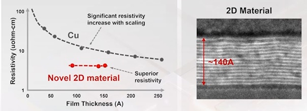
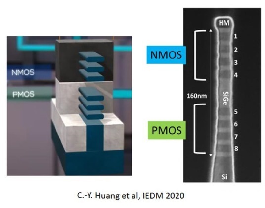
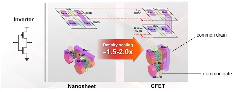
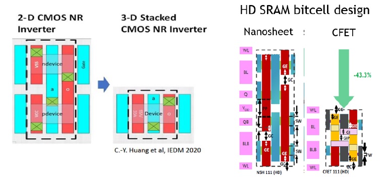
3D logic is not at all like that, since every layer is patterned. Even 3D DRAM is likely patterned at each layer. There is a vague similarity in how GAA ribbons start where the Si/SiGe layers begin as featureless uniform depositions which are then patterned and processed to open spaces around and within for the dielectrics and gates. Those initial layers, typically 6 of them, do have a multiplier effect though it is not nearly as momentus a cost reduction as the hundreds in the 3D NAND.
So, logic processes have borrowed a bit of inspiration from 3D NAND, but in most ways the processes are not compatible.