Entering a golden period of growth, mass production will begin in the second half of next year, and Nvidia is considering introducing
")
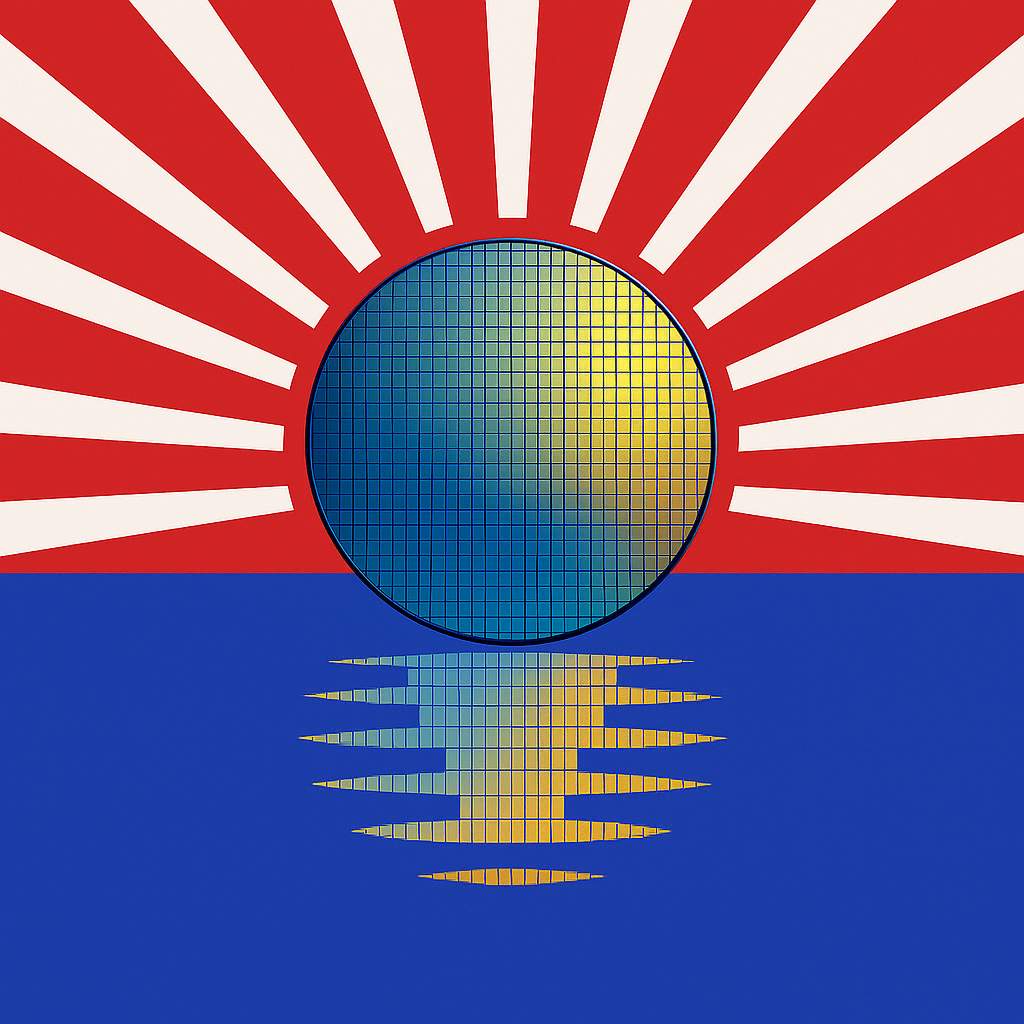
TSMC's A16, which will go into mass production in the second half of next year, will be a significant turning point in TSMC's most advanced manufacturing processes, with AI applications dominating the industry for the first time. (Photo/File photo of this newspaper)
TSMC is entering a golden age of AI growth! With its 2nm process entering mass production, HPC will drive this growth. Industry experts predict that by 2026, not only will major mobile phone manufacturers adopt TSMC's 2nm process, but AMD's 2nm HPC (high-performance computing) chips will also debut next year. Facing competition, supply chain sources indicate that Nvidia is considering adopting TSMC's most advanced process, the A16 (with a back-end powered 2nm process), which will be mass-produced in the second half of next year. This will mark a significant turning point, with AI applications dominating TSMC's cutting-edge processes for the first time.
Industry sources indicate that this marks the second time Nvidia has used TSMC's most advanced process technology for its chips since its previous 0.11-micron process. Analysts are optimistic that AI-related revenue will continue to grow, and that capital expenditures will reach new heights next year to maintain strong 2nm demand.
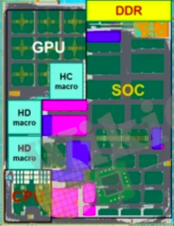
In the past, smartphones drove growth in advanced manufacturing processes, but competition has intensified in recent years. While market size has remained stable, brands are shifting their focus to peripheral products. For example, Apple has expanded its reach into in-house modems and Wi-Fi chips, such as the C1X (modem) and N1 (wireless network). Supply chain sources reveal that Nvidia is reportedly the first to introduce back-of-chip power technology, following AMD's adoption of 2nm for its Venice CPUs. This technology is expected to be used in future Feynman architectures.
Semiconductor industry analysts say that although 2nm is expensive, with Apple's 2nm chip costing nearly $27,000 each and Nvidia's back-of-chip power supply version costing more than $30,000, the significant increase in performance and chip density makes it the key reason for many customers to "pay for value."
Analysts believe that to ensure the yield of more refined processes, demand for testing and verification will increase, including SLT (system-level testing), AOI (automated optical inspection), and burn-in testing. Previously used primarily for production line monitoring, AOI will be integrated deeper into the wafer manufacturing process, achieving inspection accuracy levels beyond the reach of the naked eye. This will drive demand for related testing equipment, such as those from companies like Maktec and Huayouyi.
The AI era relies on the semiconductor industry, and TSMC has reaped the benefits of AI by leveraging its advantages in mass production and process technology.
It is reported that TSMC's sports meeting this year is scheduled to be held on November 8. At a time when revenue and profits continue to set new highs, it highlights the company's successful overcoming of challenges and creation of miracles.
 Changes in TSMC's technology platform revenue share
TSMC's A16, which will go into mass production in the second half of next year, will be a significant turning point in TSMC's most advanced manufacturing processes, with AI applications dominating the industry for the first time. (Photo/File photo of this newspaper)
TSMC is entering a golden age of AI growth! With its 2nm process entering mass production, HPC will drive this growth. Industry experts predict that by 2026, not only will major mobile phone manufacturers adopt TSMC's 2nm process, but AMD's 2nm HPC (high-performance computing) chips will also debut next year. Facing competition, supply chain sources indicate that Nvidia is considering adopting TSMC's most advanced process, the A16 (with a back-end powered 2nm process), which will be mass-produced in the second half of next year. This will mark a significant turning point, with AI applications dominating TSMC's cutting-edge processes for the first time.
Industry sources indicate that this marks the second time Nvidia has used TSMC's most advanced process technology for its chips since its previous 0.11-micron process. Analysts are optimistic that AI-related revenue will continue to grow, and that capital expenditures will reach new heights next year to maintain strong 2nm demand.
In the past, smartphones drove growth in advanced manufacturing processes, but competition has intensified in recent years. While market size has remained stable, brands are shifting their focus to peripheral products. For example, Apple has expanded its reach into in-house modems and Wi-Fi chips, such as the C1X (modem) and N1 (wireless network). Supply chain sources reveal that Nvidia is reportedly the first to introduce back-of-chip power technology, following AMD's adoption of 2nm for its Venice CPUs. This technology is expected to be used in future Feynman architectures.
Semiconductor industry analysts say that although 2nm is expensive, with Apple's 2nm chip costing nearly $27,000 each and Nvidia's back-of-chip power supply version costing more than $30,000, the significant increase in performance and chip density makes it the key reason for many customers to "pay for value."
Analysts believe that to ensure the yield of more refined processes, demand for testing and verification will increase, including SLT (system-level testing), AOI (automated optical inspection), and burn-in testing. Previously used primarily for production line monitoring, AOI will be integrated deeper into the wafer manufacturing process, achieving inspection accuracy levels beyond the reach of the naked eye. This will drive demand for related testing equipment, such as those from companies like Maktec and Huayouyi.
The AI era relies on the semiconductor industry, and TSMC has reaped the benefits of AI by leveraging its advantages in mass production and process technology.
It is reported that TSMC's sports meeting this year is scheduled to be held on November 8. At a time when revenue and profits continue to set new highs, it highlights the company's successful overcoming of challenges and creation of miracles.
Changes in TSMC's technology platform revenue share