Array
(
    [content] => 
    [params] => Array
        (
            [0] => /forum/threads/why-fdsoi.17180/page-3
        )

    [addOns] => Array
        (
            [DL6/MLTP] => 13
            [Hampel/TimeZoneDebug] => 1000070
            [SV/ChangePostDate] => 2010200
            [SemiWiki/Newsletter] => 1000010
            [SemiWiki/WPMenu] => 1000010
            [SemiWiki/XPressExtend] => 1000010
            [ThemeHouse/XLink] => 1000970
            [ThemeHouse/XPress] => 1010570
            [XF] => 2021770
            [XFI] => 1050270
        )

    [wordpress] => /var/www/html
)

Why FDSOI?

I am curious, how do you see the rise of chiplets playing out here? Does it become more interesting to keep your analog on 22FDX adjacent to an N5 digital core, and will the market evolve to support specialized processes longer term via normalizing the advanced packaging?

Perhaps that adjacent path can still be analog where the N5 does not need to drive the load, have the same ESD protection, and is not operating with such a low noise requirment, so a mm or two of trace between N5 and 22FDX literally bridges their different advantages?

We already see this playing out in optics like Ayar, partly because optical gadgets are too giant to be a good use of area on a leading edge digital process, so they seem likely to settle on chiplets with optimal processes and low cost of area.

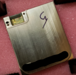
We already use 3D packaging, the 22FDX analog chips are flipped on top of a silicon photonics PIC, next to this on a common substrate is the flip-chip 5nm DSP. The RF traces between the ADC/DAC (on the DSP) and the 22FDX analog chips (on top of the PIC) are only a few mm long, bandwidth of these is >70GHz. This isn't really driven by the lower cost per mm2 of 22FDX compared to N5, but by the need to get the analog chips right next to the optical components on the PIC.
.

OE-MCM.png
 
Wow! Sounds like the highest end transceiver. It must require extremely low jitter time slices. Do you go with a PLL with an inductor? If yes, would you put the inductor onto the main substrate/interposer?

Anybody want to speculate what NRE would be just to prototype this, assuming you can MPW the die and package it as Ian is describing.
The one in the photo -- there are >100k of them out there now -- is a 400G coherent transceiver -- and you're right, jitter is of the order of 100fs. PLL inductor is on-chip, frequency is too high for off-chip.

Most of the NRE is the design/development cost of the chips not prototyping the MCM -- though this is of course neither simple nor cheap in itself, the DSP probably dominates, and there are various numbers out there for the cost of 7nm/5nm chips... ;-)

P.S. Not the highest end any more, here's a 1.2T one... :)
 

Attachments

  • coh1p2T.png
    coh1p2T.png
    211.4 KB · Views: 265
This is insane. This must be for a tower.

I don't think you can pass the 250fs jitter barrier with a simple ring oscillator, but you would know more than me. I hear that the jitter barrier for an inductor style VCO is about 50f, so 100f is pretty good. How would you measure the jitter? Built-in histograms? The built-in diagnostics must be a huge effort.

Engineer salary costs.. yes, that would be the biggie. Any ballpark on the ratio between RF/analog designers vs DSP engineers? Do the engineers handle their own layouts?
 
This is a really great thread, thanks for sharing guys!

For prototyping: PIC and 22FDX can easily be MPW'd through Europractice, prices are published publicly. The DSP is in a league of its own but there are many commercial coherent 5nm DSPs ^^
 
I only mentioned "MPW" so that you guys wouldn't add the full mask costs to the NRE. I will really asking about the engineering labor and the EDA costs.
 
I am trying to figure out how many engineers are needed for a transceiver design team. I am familiar with 2 transceiver teams in the US. Ian is likely to be on the tower (high end) side. I am also interested in local transceivers (1ns jitter, 16-12nm), and would like to see if it is possible to bring the NRE cost down below $5M. This assumes the senior circuit designers are in complete control, the layouts are semiautomated, and the parasitics are available on the fly.
 
This is insane. This must be for a tower.

I don't think you can pass the 250fs jitter barrier with a simple ring oscillator, but you would know more than me. I hear that the jitter barrier for an inductor style VCO is about 50f, so 100f is pretty good. How would you measure the jitter? Built-in histograms? The built-in diagnostics must be a huge effort.

Engineer salary costs.. yes, that would be the biggie. Any ballpark on the ratio between RF/analog designers vs DSP engineers? Do the engineers handle their own layouts?
They're for optical fiber networks in the internet backbone, reach can be anywhere between 10km to 10000km depending on application.

Jitter is measured with a phase noise/jitter analyser, these can easily measure down to 5fs.

Don't know what the ratio between analog/RF and digital is, design teams are spread across 5 different locations in 3 continents. For advanced work the engineers do their own layouts, some of the easier stuff is done by in-house or contracted layout engineers -- there are so many tradeoffs for high-end analogue it's very difficult to write a specification that can be handed over, and can take the designer as long to explain (and review, and fix...) the layout as it does to do it. Also the layout often needs optimizing (e.g. to reduce parasitics or coupling) to get best performance, and the designer needs to do this.
 
Last edited:
I am trying to figure out how many engineers are needed for a transceiver design team. I am familiar with 2 transceiver teams in the US. Ian is likely to be on the tower (high end) side. I am also interested in local transceivers (1ns jitter, 16-12nm), and would like to see if it is possible to bring the NRE cost down below $5M. This assumes the senior circuit designers are in complete control, the layouts are semiautomated, and the parasitics are available on the fly.
That's like asking how long a piece of string is. The effort depends very heavily on the type of transciever and the channel it has to drive, for example a long-reach 112G PAM4 transceiver is *way* more complex and needs *far* more design effort than a short-reach 16G one.
 
You can create the example that you would know about. For example, you mentioned PAM4 112G. Alpha Wave has videos on YouTube probably similar to the specs you have in mind. I mentioned "the senior circuit designers are in complete control, the layouts are semiautomated, and the parasitics are available on the fly".

"Design teams are spread across 5 different locations in 3 continents" ... what is the relevance?

I can't give any numbers (team size/design cost) for obvious reasons, so I was kind of hinting that this isn't something you can do with a handful of engineers and a small budget, unless it's a simple low-speed transceiver ;-)

To give you an idea, IIRC the license fee in $ for a leading-edge high-speed transceiver in an advanced process from someone like Synopsys (or Alphawave?) has 8 digits...
 
Last edited:
I believe it is around 50 engineers in a flat organization. 267 once you start adding middle management. At Intel, the numbers would be higher, but Mr. Blue would need to do that calculation.
 
Back
Top