These indicated 14nm (i.e., Samsung).
Array
(
    [content] =>
    [params] => Array
        (
            [0] => /forum/threads/youre-fabbing-it-wrong-chip-shortages-due-to-lack-of-investment-in-the-right-factories-says-idc.15391/page-2
        )

    [addOns] => Array
        (
            [DL6/MLTP] => 13
            [Hampel/TimeZoneDebug] => 1000070
            [SV/ChangePostDate] => 2010200
            [SemiWiki/EmailDomainReplace] => 1000010
            [SemiWiki/Newsletter] => 1000010
            [SemiWiki/WPMenu] => 1000010
            [SemiWiki/XPressExtend] => 1000010
            [ThemeHouse/XLink] => 1000970
            [ThemeHouse/XPress] => 1010570
            [XF] => 2031070
            [XFI] => 1060170
        )

    [wordpress] => /var/www/html
)
Guests have limited access.
Join our community today!
Join our community today!
You are currently viewing SemiWiki as a guest which gives you limited access to the site. To view blog comments and experience other SemiWiki features you must be a registered member. Registration is fast, simple, and absolutely free so please, join our community today!
You are using an out of date browser. It may not display this or other websites correctly.
You should upgrade or use an alternative browser.
You should upgrade or use an alternative browser.
You're fabbing it wrong: Chip shortages due to lack of investment in the right factories, says IDC
- Thread starter soAsian
- Start date
Too expensive. Anything 1m/year< will never leave 130nm-180nm because of lot sizes.
For most of mortals, a tapeout on 200mm is the only thing they can hope for in their lifetime.
Design of physical IP on immersion nodes is too expensive too. It's not what 10 years old pirated Cadence can do, nor what Indian, or Bangladeshi VHDL outsourcing shops specialise on.
Very true which is why the automotive companies all use the same off-the-shelf chips that they can can't get right now. Well, there will be plenty of room @ 28nm for those who can afford it:
Recent UMC call:
"On the supply side, based on the announced capacity expansion plan, we do see the oversupply situation at 28nm to happen beyond 2023, not before 2023," Jason Wong, president of UMC, told analysts on the call.
This automobile chip shortage is a bubble. We had enough manufacturing capacity before the pandemic and we have enough now so stop the shortage narrative already. Look at TSMC's automotive numbers for 2019 (-7%), 2020 (-7%), and 2021 (+51%). Give it another year and we will be caught up, especially if inflation keeps going and consumer spending slows.
Can somebody tell me how many cars are sold per year over the last five years? Has it really changed that much? And yes cars have more chips in them but it takes longer to design a car than to build a fab so how about some planning for the future? That the good thing about systems companies. They have plenty of time to forecast chip supply and demand, assuming they get the demand right.
The car companies really need to start designing out the old chips and designing in new ones like Tesla and the other emerging car companies. Learn the lesson of the business dinosaurs already: Innovate or Die.
jms_embedded
Well-known member
The car companies really need to start designing out the old chips and designing in new ones like Tesla and the other emerging car companies. Learn the lesson of the business dinosaurs already: Innovate or Die.
Daniel, I respect your experience in the industry, but you keep saying that, and yet there are technical and economic reasons why 40nm+ nodes are still used throughout today's car. (And I'd be willing to bet this includes Tesla.)
I am wondering which ICs you are referring to? All ICs in an automobile? Some large subset of them? Just the major ones?
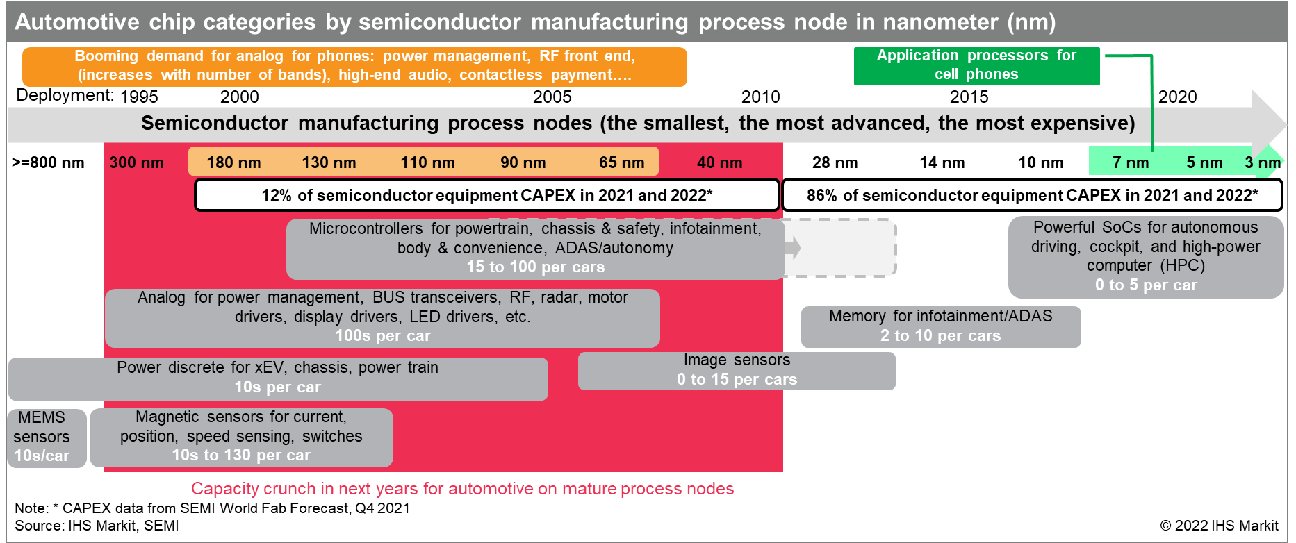
This recent diagram from IHS Markit was really informative to me, and consistent with what I've been reading about from many sources:
We are starting to see some of the larger MCUs migrating to 28nm and smaller geometries: search for "28nm automotive" and it pulls up lots of Renesas references, and it looks like Infineon AURIX TC4x is 28nm. And NXP even has a 16nm automotive IC (S32) for ADAS.... but it's $38 at 1k quantity. (And if you read the fine print, it has SRAM but the program memory needs to be pulled in from an external quad-SPI NOR or eMMC NAND flash chip. See development board PDF. Not sure what kind of cost adder that is. Mouser has some 32MB NOR flash chips from Dialog Semiconductor at 66c in 6K quantity but those are -40 to +85 C, not automotive grade.)
There are tons of "jellybean" ICs scattered throughout cars, including analog and microcontrollers, which are lower cost, and are apparently on larger geometry nodes because the economics don't work to put them on smaller geometry nodes. A car is not a single-chip SOC solution.
I do think we're likely to see some more integration (pulling analog + CAN/LIN transceivers and other functionalities into MCUs) which would help justify going to a smaller geometry, but unless there's some critical complexity level reached, the math doesn't work to reach 28nm. I don't know what that number is, since I'm not privy to cost-modeling information, but I am very confident it is there.
I guess one question is who can do it more cost-effectively, the existing microcontroller manufacturers with a more general-purpose IC (with a variety of customers to increase volumes, but they need to meet their markup requirements) or the automotive manufacturers as system integrators with a more special purpose IC they design directly (and therefore less markup needed for meeting cost targets, but less volume than a fab-lite microcontroller manufacturers).
Daniel, I respect your experience in the industry, but you keep saying that, and yet there are technical and economic reasons why 40nm+ nodes are still used throughout today's car. (And I'd be willing to bet this includes Tesla.) I am wondering which ICs you are referring to? All ICs in an automobile? Some large subset of them? Just the major ones?
Think about how cars evolved. My first car had no chips. Then came electronic fuel injection and other automotive systems went digital but remained independent. Before ADAS cars had no real brain, no central control system. Tesla changed that and brought systems together with a massive amount of software and integration. At first Tesla used NVIDIA and Mobileye and other off the shelf chips that they cobbled together. Now Tesla is moving up the autonomous roadmap through highly integrated custom silicon and software that requires an incredible amount of compute power. Once they hit AV level 5 it will be a truly integrated system of leading edge silicon (300mm).
You can't look at what's in the majority of cars today. Look at automotive innovation before Tesla came about. We had hybrid EVs and no autonomy. You can look at all the automotive history chip charts you can google up but if you want to see the future of automotive silicon look at TSMC and Tesla. There is a reason TSMC quickly qualified N5 for automotive because that is the future. There is a reason why Tesla is breaking automotive technology barriers left and right because that is the future.
I remember when Apple decided to do their own SoC. Qualcomm said who can do it better the existing dominant SoC vendor with many customers or a fruity computer company. We now know the answer to that.
I believe this for high-volume ICs that aren't low-cost. What kind of mask set costs (rough order of magnitude) are we talking about for 28nm?
IDK what the semiconductor companies need to justify producing a new IC in the $1-$2 range (high volume cost to customer) but I suspect the one-time costs for design and production need to be amortized over expected volume to be less than 20 cents*. (For required gross margin / operating margin, look at recent earnings reports.)
(*yes I work for a certain semiconductor manufacturer, no I do not work in IC design or production; this is a vague guess given that I don't want to find out a real number and deal with confidentiality constraints.)
28nm set made up of how many masks?
Indeed, NOR flash on the microcontroller does not scale beyond 40nm foundry node (~60-70 nm active width). The high-k CMOS option of 28nm is a popular option (for a given cell size).The challenge has been eNVM on these nodes; 40nm eFlash qual for Auto was in 2018 (https://www.tsmc.com/english/dedicatedFoundry/technology/specialty/eflash), and the cycle time for auto components is ~3 years for the platform certification and then a ~10 year support lifetime commit from the manufacturer. So anyone that was designing a "new car" platform in 2019 would not have considered anything less than 40nm as appropriate if including eNVM. Renesas worked on porting their MONOS Flash to 28nm, and that was supposed to be ramping in 2020 (https://www.renesas.com/us/en/about...boration-next-generation-green-and-autonomous) - no idea if that panned out. N28/22 for Wireless / IoT applications with eNVM was focused on STT-MRAM or RRAM rather than eFlash, and the former has challenges with magnetics (so not going into any ECU), and the latter performance / endurance may not meet the spec of the part (incl temp range). If one were designing a new part in 2021/22 expected to launch in '24-'25 timeframe, then I would agree that 28nm is a good option, but their capacity is not limitless either - that's why they are expanding into Japan, to support the Sony ISP business.
Unrelated, but interesting was a paper from TSMC at VLSI in 2019 (I think) that showed their Wafer-on-Wafer attach putting a N40 die with eFlash atop an N16 logic die, specifically to bring that eNVM capability to a more advanced node, b/c the only current eNVMs for FinFET are still STT/SOT or RRAM based.
Last edited:
hist78
Well-known member
Will MPW (multi-project wafer) be possible and partially resolve the small lot size dilemmas?Too expensive. Anything 1m/year< will never leave 130nm-180nm because of lot sizes.
For most of mortals, a tapeout on 200mm is the only thing they can hope for in their lifetime.
Design of physical IP on immersion nodes is too expensive too. It's not what 10 years old pirated Cadence can do, nor what Indian, or Bangladeshi VHDL outsourcing shops specialise on.
Will MPW (multi-project wafer) be possible and partially resolve the small lot size dilemmas?
No, nobody will do this for real commercial use, especially for analog, where per-design process variation is needed. I doubt a 300mm MPW can be spun for non-academic, and non-test runs.
MPW is very inflexible for mainstream commercial use. Basically, you lose nearly all ability to say, when, and how much dies you want.
hist78
Well-known member
No, nobody will do this for real commercial use, especially for analog, where per-design process variation is needed. I doubt a 300mm MPW can be spun for non-academic, and non-test runs.
MPW is very inflexible for mainstream commercial use. Basically, you lose nearly all ability to say, when, and how much dies you want.
Is there any other options available other than waiting for new fabs and additional fab capacity come online in two to three years to resolve the chip shortage?
The challenge has been eNVM on these nodes; 40nm eFlash qual for Auto was in 2018 (https://www.tsmc.com/english/dedicatedFoundry/technology/specialty/eflash), and the cycle time for auto components is ~3 years for the platform certification and then a ~10 year support lifetime commit from the manufacturer. So anyone that was designing a "new car" platform in 2019 would not have considered anything less than 40nm as appropriate if including eNVM. Renesas worked on porting their MONOS Flash to 28nm, and that was supposed to be ramping in 2020 (https://www.renesas.com/us/en/about...boration-next-generation-green-and-autonomous) - no idea if that panned out. N28/22 for Wireless / IoT applications with eNVM was focused on STT-MRAM or RRAM rather than eFlash, and the former has challenges with magnetics (so not going into any ECU), and the latter performance / endurance may not meet the spec of the part (incl temp range). If one were designing a new part in 2021/22 expected to launch in '24-'25 timeframe, then I would agree that 28nm is a good option, but their capacity is not limitless either - that's why they are expanding into Japan, to support the Sony ISP business.
Unrelated, but interesting was a paper from TSMC at VLSI in 2019 (I think) that showed their Wafer-on-Wafer attach putting a N40 die with eFlash atop an N16 logic die, specifically to bring that eNVM capability to a more advanced node, b/c the only current eNVMs for FinFET are still STT/SOT or RRAM based.
A buddy of mine was working on exactly the same task: a cheap way to stack MCU dies with memory without TSVs, and expensive hybrid bonding, except doing it for SRAM instead of eFlash.
The idiocy of modern MCU design is that if you open a top-tier, fancy MCU on new nodes, you will find that 90% of the die is just huge eFLASH, and SRAM + tiny, tiny MCU core, and huge analog circuitry. So, on new nodes, actual core takes just few percents of the die space, and only these few percents of the area do get benefit from lower nodes. Everything else is negative value for the MCU.
Basically, MCU makers have turned into flash, and SRAM makers, and they are using suboptimal design, and process for both of them.
Last edited:
Is there any other options available other than waiting for new fabs and additional fab capacity come online in two to three years to resolve the chip shortage?
No, no real new 200mm fabs coming. SMIC was the last 200mm player with new equipment, and everybody were saying they were crazy. Now they haul money by the bucket.
There are few scrawny players now trying to replicate the SMIC thing too. They bought the last of second hand 200mm tools available on the market, some even try offering a commercial service on a single stepper.
A buddy of mine was working on exactly the same task: a cheap way to stack MCU dies with memory without TSVs, and expensive hybrid bonding, except doing it for SRAM instead of eFlash.
The idiocy of modern MCU design is that if you open a top-tier, fancy MCU on new nodes, you will find that 90% of the die is just huge eFLASH, and SRAM + tiny, tiny MCU core, and huge analog circuitry. So, on new nodes, actual core takes just few percents of the die space, and only these few percents of the area do get benefit from lower nodes. Everything else is negative value for the MCU.
@Fred Chen
That could be a golden goose for WinBond to pick. My friend gave up on the venture, as he got better funded projects coming. He was looking into inductive interconnect back to back, or through with wafer thinning.
Inductive interconnect avoids expensive TSV's and allows use of dissimilar size dies without dummy silicon. I think he also experimented with capacitive one, which takes more space, but is needs even less stacking precision.