AI was everywhere at DAC. Presentations, panel discussions, research papers and poster sessions all had a strong dose of AI. At the DAC Pavillion on Monday two heavy weights in the industry, Siemens and NVIDIA took the stage to discuss AI for design, both present and future. What made this event stand out for me was the substantial dose of real results and grounded analysis of where it was all going. Both speakers did a great job, with lots of real data. Let’s look at what was presented in the DAC TechTalk – A Siemens and NVIDIA perspective on unlocking the power of AI in EDA.
The Presenters

There were two excellent presenters at this event.
Amit Gupta is a technology executive and serial entrepreneur with over two decades of leadership in semiconductor design automation and AI innovation. At Siemens EDA, Amit leads the Custom IC division and spearheads AI initiatives across the organization. I attended several events where Amit was participating at DAC. He has an easy-going style that is deeply grounded in real-world experience. He’s a pleasure to listen to and his comments are hard to ignore.

Dr. John Linford leads NVIDIA’s CAE/EDA product team. John’s experience spans high-performance physical simulation, extreme-scale software optimization, software performance analysis and projection, and pre-silicon simulation and design. Before NVIDIA, John worked at Arm Ltd. where he helped develop the Arm software ecosystem for cloud and HPC. John brought specific, real examples of how NVIDIA is fueling the AI revolution for Siemens and others.
The Siemens Perspective
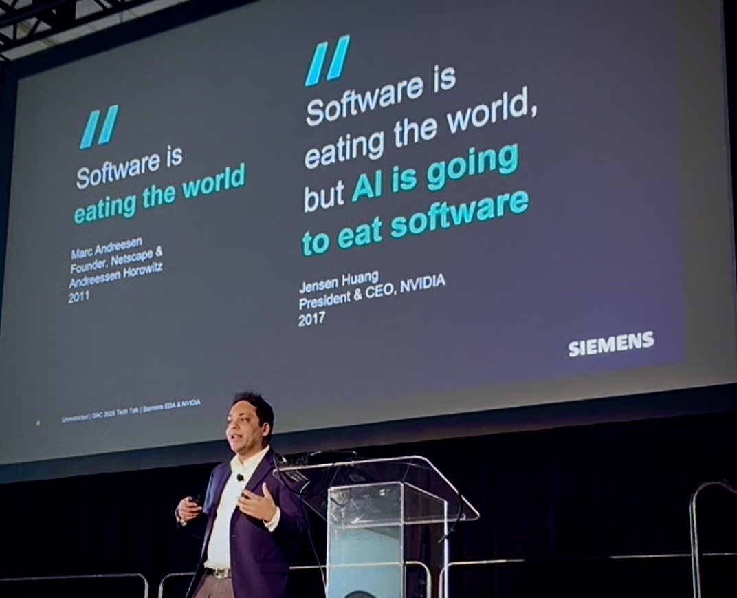
Amit kicked off the presentation by taking a rather famous quote and updating it with NVIDIA’S perspective as shown in the image at the top of this post. It was appropriate for NVIDIA to weigh in on this topic as they are enabling a lot of the changes we see around us. More on that in a moment.
Amit began by observing the incredible growth the semiconductor market has experienced, due in large part to the demands of AI. The semiconductor market is projected to hit one trillion dollars by 2030. Amit pointed out that the growth from about one hundred billion to one trillion dollars took several decades, but the growth from one trillion to two trillion dollars is projected to take about 10 years. The acceleration is accelerating if you will.
This fast growth brings to mind another eye-catching statistic. It took several decades starting in the late 1940’s to sell the first one million TV sets. After the launch of the iPhone is 2007, it took Apple just 74 days to sell one million of them. The adoption of new technology is clearly accelerating. Amit cited statistics that demonstrate how the industry is moving toward a software-defined, AI powered, silicon enabled environment of purpose-built silicon to drive the differentiation of AI workloads. This is the new system design paradigm and the new role of semiconductors. These are the tasks that Siemens EDA is focusing on, both for chips and PCBs.
Amit described the dramatic increase in design complexity, demands for decreased time to market and the lack of engineering talent to keep up. It is against this backdrop that AI holds great promise. He described the broad footprint of investment Siemens EDA is making across many AI disciplines, as shown in the figure below.

He explained that each discipline has a specific impact, with those on the left generally making tools more efficient with reduced run time and improved quality of results while those on the right make it easier and more efficient to interact with the tools using natural language to set up complex runs. This is where the lack of engineering expertise can be mitigated. Amit referred to a major announcement Siemens made at DAC describing its EDA System to enable advanced AI and UI capabilities across the entire product line. Details of the Siemens EDA AI announcement can be found on SemiWiki here.
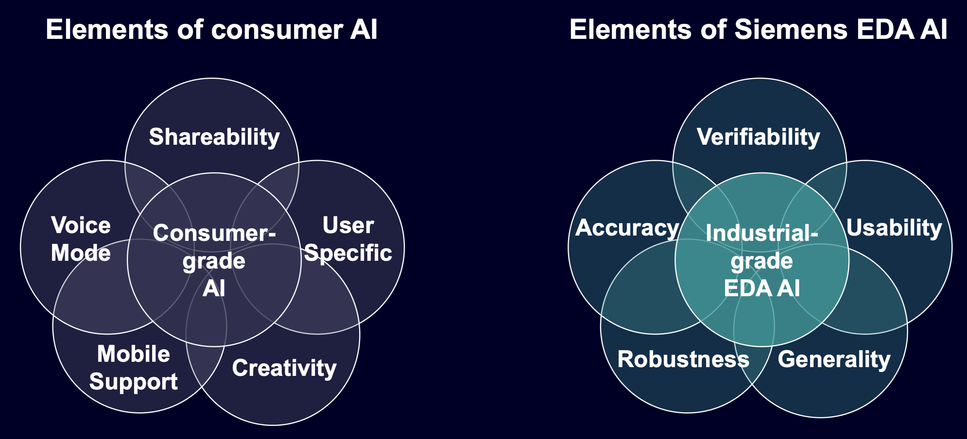
Amit then illustrated the special needs of EDA AI. This is an area where he is particularly well versed as his prior company, Solido was using AI for over 20 years. It turns out there is a big difference between consumer AI and EDA AI. Amit ran some live examples to illustrate how consumer grade AI will simply not work for chip design tasks. The figure below illustrates some of the ways these two tasks have very different requirements.

This is the essence of why Siemens EDA AI is so effective. Amit explained that beyond the image and language processing delivered by consumer AI, there is a need to master elements such as technical documentation, script generation, creating test benches, and specific design formats such as Verilog and GDSII. He described the Siemens EDA AI system as the “connective tissue” for chip and board design.
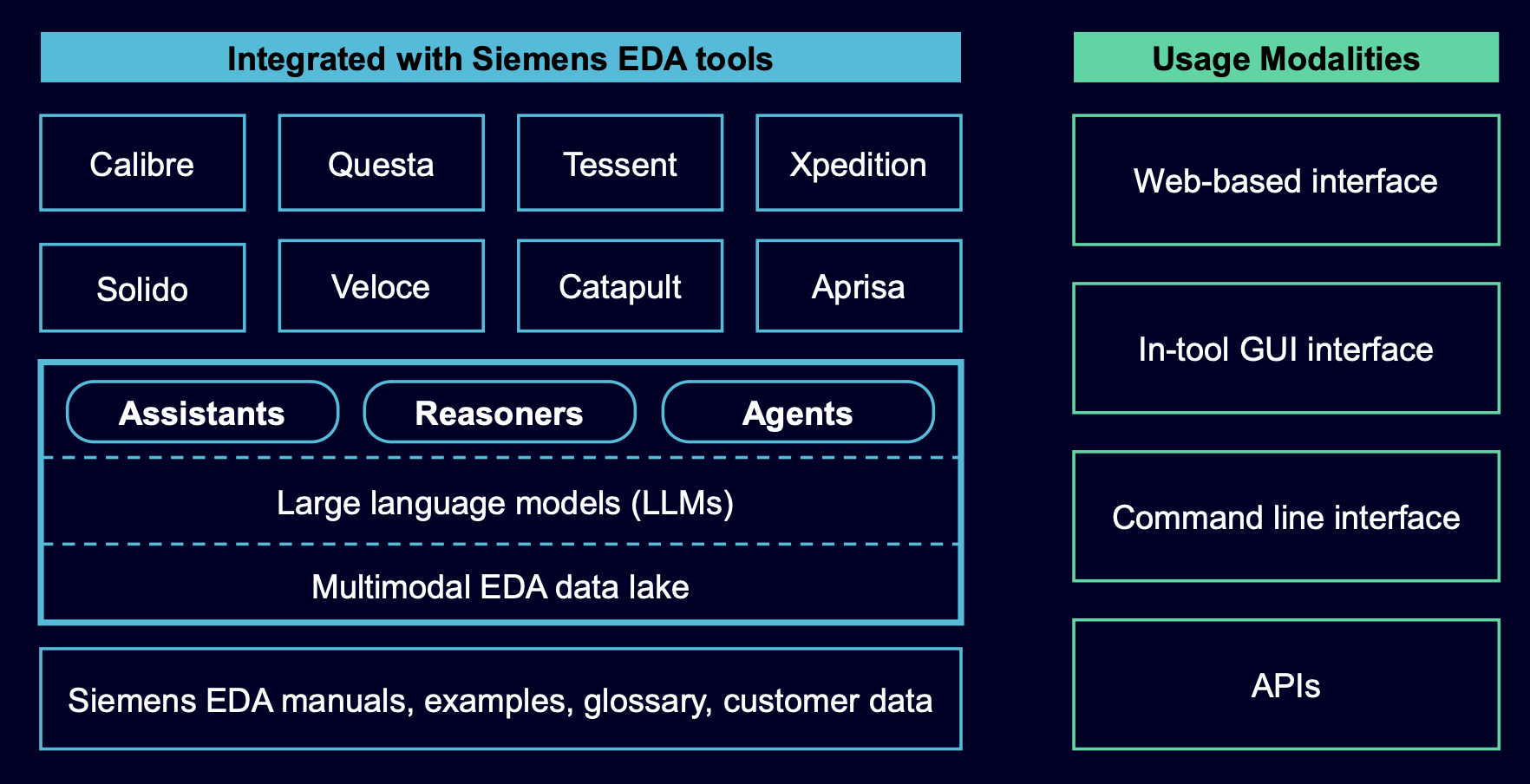
Amit described how the Siemens EDA AI System enables generative and agentic AI across the EDA workflow. This is an aggressive program that enables many parts of the Siemens EDA portfolio with new, state-of-the-art capabilities. The diagram below provides an overview of the system’s impact.

Amit then introduced Dr. John Linford to describe how NVIDIA and Siemens are partnering at the hardware, AI model and microservices levels.
The NVIDIA Perspective
John began by explaining how NVIDIA builds supercomputing infrastructure that is co-designed with the software, networks, CPUs, and GPUs, all brought together into an integrated platform that is used by NVIDIA to design its own chips. This system is then sold either in parts or completely to others to enable a broad community to also develop advanced solutions. This recursive model represents some of the elements of NVIDIA’s success and informs how NVIDIA collaborates with Siemens to help create its EDA AI framework.
John described how NVIDIA enables innovation across many areas, both software and hardware. He began by describing the breadth of the CUDA-X libraries, which form a foundational element for NVIDIA. These libraries deliver domain-specific accelerated computing across approximately 450 areas. As examples, there are libraries focused on chip lithography, computational acceleration for tasks such as fluid dynamics and thermal/electrical analysis, and even interfaces to allow the creation of new accelerators for tasks such as physical analysis.
He went on to describe agentic AI workflows that help to accelerate the designer’s creative work as well as quality control and yield management. John then touched on NVIDIA NeMo, a Python-based framework that allows the development of enterprise-grade agentic AI solutions, from data acquisition and curation, to training and deployment, to guardrail analysis. This is an example of some of the capabilities that Siemens can use to build its AI solutions. He also explained now NVIDIA inference microservices, or NIM delivers the building blocks for deployment of complete AI solutions, either in the cloud or on premises.
John also described how NVIDIA accelerates physical simulation, replacing massive explicit analysis with inference to find solutions much faster. This application finds a good match for digital twin development. These solutions don’t necessarily replace long, first-principal analysis but the trained models and inference get you to the final answer to verify much faster.
To Learn More
This presentation provided excellent detail behind the Siemens EDA AI announcement. This work promises to have a substantial impact on design quality and productivity for complex chip and PCB design. NVIDIA also appears to be well-positioned to provide proven, targeted hardware and software to help realize these innovations.
If complex, AI-fueled design is in your future, you need to take a close look at what Siemens is up to. You can read the full press release announcing the Siemens EDA AI work here. And you can get a broader view of the Siemens EDA AI work here. And while you’re at it, check out this short but very informative video on how AI is impacting semiconductor design.
And that’s the DAC TechTalk – A Siemens and NVIDIA perspective on unlocking the power of AI in EDA.
Share this post via:


Comments
There are no comments yet.
You must register or log in to view/post comments.