- This event has passed.
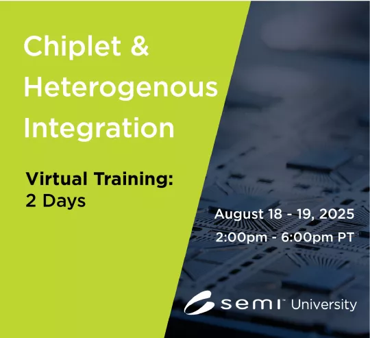
Chiplet and Heterogeneous Integration for Microelectronics Packaging – Virtual Training

Chiplet and heterogeneous integration of packaging has been embraced as the next revolutionary innovation to meet the quest of size, cost, and performance for packaging. The technologies are seen as another disruptive technology to bring devices into a package by integrating the various Multi-chip module (MCM), 3D packaging, Through Silicon Via (TSV), and Fan-out wafer level packaging (Fo-WLP) technologies into a system in the package for applications. Chiplet, EMIB, and glass substrate will also be shared in this course.
Pricing
- Members: $599
- Non-Members: $649
* For group orders with 10+ attendees, and for Students/Veterans discounted pricing, please contact semiu-support@semi.org.
Time
2:00 pm – 6:00 pm PDT
Course Description
This workshop reviews the needs of the packaging solution to meet the demand for digitalization through the artificial intelligent and Internet-of-things from urbanization, sustainability to industry. The course provides an overview of the fabrication process of IC carriers of leadframe, ceramics, substrate and flex and how they have to evolve to meet the heterogeneous integration. With these foundations, various stacking and integration technologies through wirebonding, flip chip and 3D interconnect from interconnect to system level will be shared. Packaging innovation of TSV, fan-in, fan-out wafer level packaging and its challenges will also be shared for chiplet and heterogeneous integration. It ends off by sharing the embedded technologies and embedded multi-die interconnect bridge for chiplet and heterogeneous integration.
The course looks into the R&D development as well as the dynamics changes of heterogeneous integration technologies in the Semiconductor packaging arena. This workshop curates the technologies development to date and provides the necessary information for professionals in the manufacturing and R&D environment to perform their tasks.
Who Should Attend
This course is intended for both manufacturing and R&D know-how in IC packaging professionals, including but not limited to:
- Directors
- Managers
- Process Engineers
- R&D Engineers
- Sales and Application Engineers who supply packaging materials and tools
Learning Objectives
- Understand why chiplet and heterogeneous integration for advanced packaging
- Review of IC carriers
- Summarize 3D and TSV for Chiplet and Heterogeneous Integration
- Explain Fan-in and Fan-out wafer-level packaging for chiplet and heterogeneous integration
- Describe chiplet, embedded, and embedded multi-die interconnect beam for chiplet and glass substrate for heterogenous integration
Instructor

Dr. Lee Teck Kheng
Institue of Technical Education
Important Information
Note that only the person who registered will receive a certificate of completion. This virtual training will not be recorded. Attendees must be present to access course knowledge.
Can’t find the training link day of? After you register, you will receive the link to the live training via the email address you provided. In addition, you will receive email reminders about 24 hours in an advance and an hour before with the same link. Please keep these emails on hand to access the trainings on time. If you do not see any confirmation emails, please check your junk/spam folders before contacting SEMI U for support.


Intel to Compete with Broadcom and Marvell in the Lucrative ASIC Business