As of today NVM IP has been mostly used in SoC or IC to support very specific needs like analog trimming and calibration or encryption key integration for Digital Right Management (DRM) purpose. In other words small size (less than 1K-bit) few times programmable (FTP) NVM IP was enough to support these needs, thus most of the NVM IP market was based on this type of memories, based on antifuse technology or equivalent One Time Programmable (OTP) or FTP when redundancy was inserted to offer more than one programmable capability. This was only a portion of the market need, as if you look at Flash application spectrum, most of it is made of MCU (CPU) code support.
The above mentioned technologies are not cost effective to support on-chip code integration, for two main reasons. At first, if you launch a MCU with on-chip code, your customer will expect to be able to change the program many times, not just a few times. Moreover, as the same customer expect to integrate enough NVM to support the MCU code, the FTP solution quickly lead to a far too large IP block. If the need for on-chip NVM is really crucial, you may want to look at using an Embedded Flash CMOS technology. But if you target a cost sensitive application, the chip cost will be impacted by the high number of extra mask levels to support Embedded Flash CMOS process, leading to (25% or more) higher chip price…

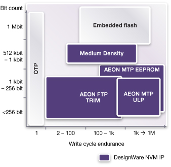
The DesignWare NVM IP port-folio above pictured shows that the “Medium Density” solution just announced by Synopsys should be the best fit if you search for NVM IP able to support MCU code, offering decent write cycle endurance (1K cycles or more) as well as code size up to 64 K-bit and still based on standard CMOS technology. Because this NVM family is based on a completely new architecture, the cell density is 5X better over lower bit count solutions. The Flash access time is less than 40 ns, well positioned to support low power MCU used in IoT for example. Automotive is also a target market for this NVM, so ECC has been added for reliability and the data retention is guaranteed for 10 years… at 125 C.
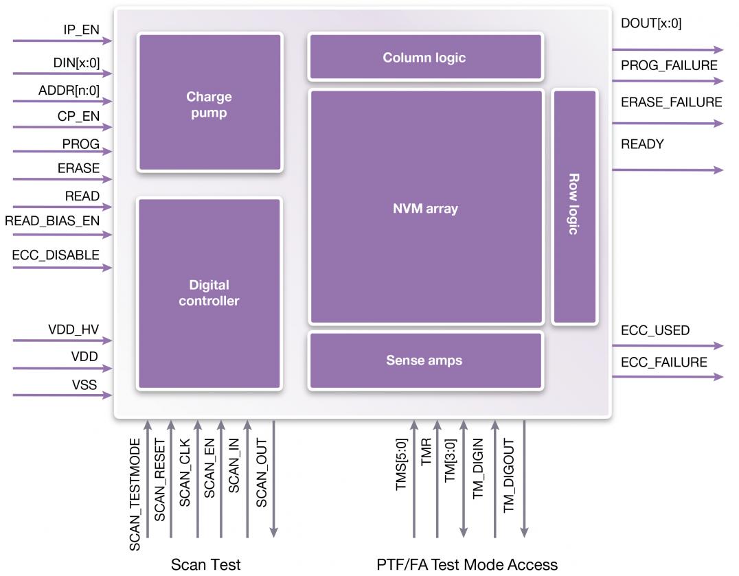
The high voltage circuitry (charge pump) and the memory array digital control is part of the IP, to ease designer life.

I have focused on MCU code application, in fact such Medium Density NVM IP target is mostly analog IC like:
- Smart sensors
- Power Management
- Touchscreen controllers
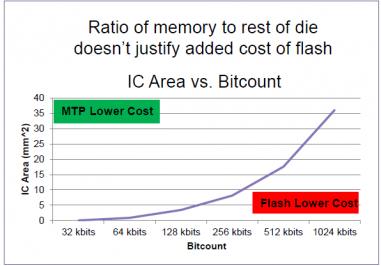
But the trend is to integrate microcontroller into Analog ICs, thus this NVM IP is expected to be massively used in the analog market segment. If you need to be convinced that NVM IP is a more cost effective solution, just take a look at the picture below: the curve is representing the IC area function of the bit count. When the IC is small and the flash complexity is very high (say above 256 kbits), embedded flash is better. But for most of the chips MTP is more cost effective (the largest part of the diagram area, on the left side).

More information about the new DesignWare® Medium Density Non-Volatile Memory (NVM) IP family.
From Eric Esteve from IPNEST
Share this post via:


Comments
There are no comments yet.
You must register or log in to view/post comments.