When most people hear the term PDF, they immediately think of a PDF file, a universal, platform-independent way to share electronic documents.
There is, however, another PDF that many outside the semiconductor industry may not be familiar with. And this PDF actually predates the PDF file format. It is short for PDF Solutions, a company whose software platforms are widely used across the semiconductor ecosystem, from design through manufacturing and test.
While the company does not formally expand the initials “PDF,” they can be logically interpreted as Process, Design, and Fabrication, reflecting its long-standing mission to connect design intent with manufacturing reality using silicon data. As Qualcomm’s Mike Campbell has described them, the software tools offered by PDF Solutions have become “the industry’s tools,” underscoring how deeply embedded they are across leading semiconductor companies.
PDF Solutions held its annual User Conference earlier in December, and the following article provides a synthesis of the key themes, technologies, and customer perspectives presented at the event.
The industry’s new reality
Explosive demand for AI, data center, and edge workloads is driving aggressive investment in advanced nodes, chiplets, and 3D integration, pushing semiconductor revenues toward the low-trillion-dollar range before 2030. At the same time, the move to sub-2 nm processes, multi-die systems, and globally distributed manufacturing has shifted the industry’s core challenge from linear scaling to systemic complexity.
Yield, cost, and cycle time are no longer determined within a single fab or toolset. They depend on tightly coupled decisions across design, front-end manufacturing, advanced packaging, final test, and a supply chain that spans continents. More fabs are coming online, more test insertions are required per device, and more data is being generated at every step. Yet only a small fraction of that data is actively analyzed using conventional approaches.
Traditional economies of scale are increasingly difficult to realize in this environment. Operations are fragmented across sites and companies, experienced talent is constrained, and data lives in incompatible schemas and tools that make holistic analysis slow and expert-dependent.
Why AI-driven collaboration is becoming essential
Across the industry, AI is now applied to yield optimization, predictive maintenance, planning, and logistics. However, as discussed at the User Conference, its impact remains limited when data is locked in silos or when AI initiatives stall at the proof-of-concept stage rather than becoming operational systems.
In semiconductor manufacturing, a disproportionate amount of data-science effort is still consumed by data preparation rather than modeling or decision-making. Many AI projects fail not because algorithms are inadequate, but because they lack robust data foundations, governance, and deployment pathways.

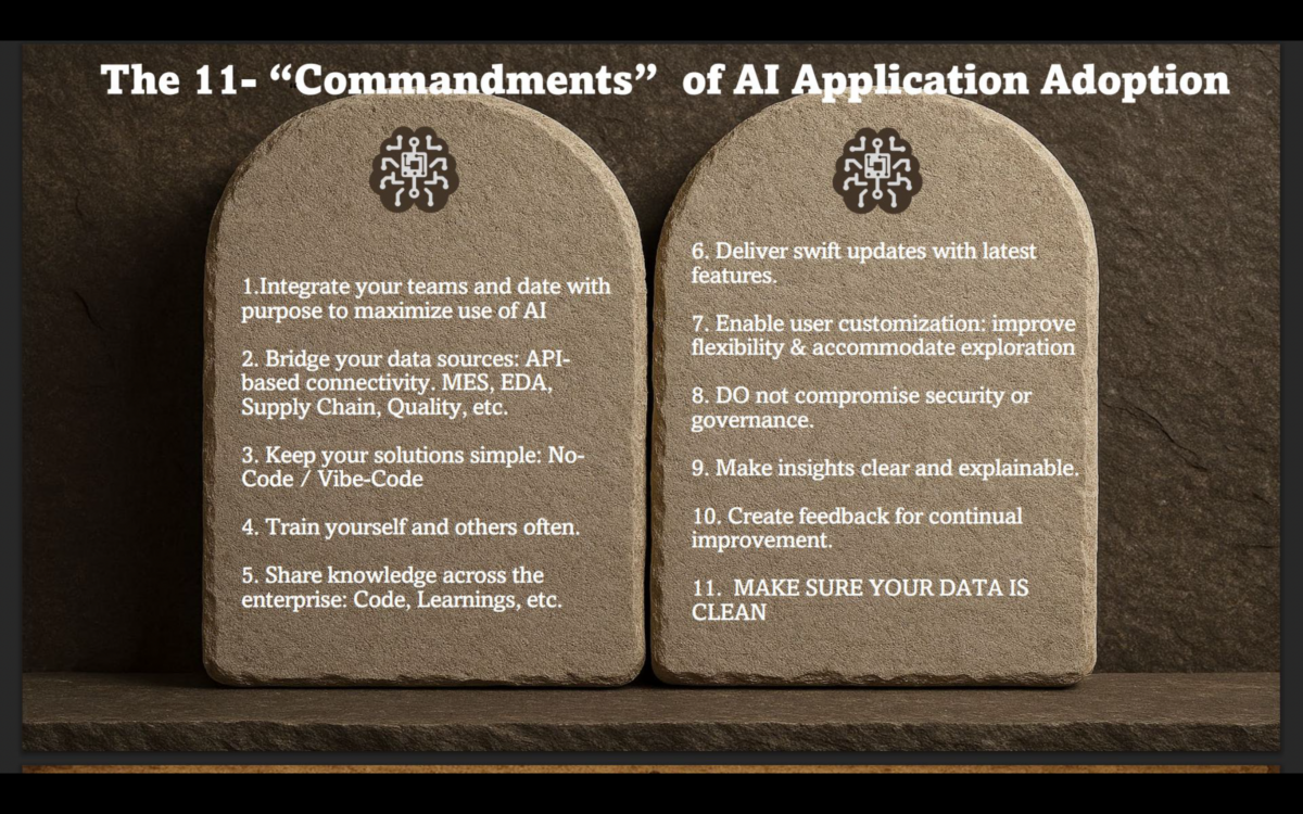
Source: Adapted from Michael Campbell’s presentation at the 2025 PDF Solutions Users Conference.
From John Kibarian’s perspective, the next major wave of value, potentially in the hundreds of billions of dollars annually at an industry level, will come from AI-driven collaboration across the semiconductor ecosystem, not isolated point optimizations. Realizing that value requires secure, standards-based connectivity, AI-ready data platforms, and workflows that link design, manufacturing, test, and supply-chain decisions into a continuous, data-backed loop.
PDF Solutions’ AI strategy
The strategy rests on three reinforcing pillars: enterprise-grade ModelOps, deep data integration with semiconductor-specific semantics, and a secure, LLM-based agentic workflow platform designed for high-stakes manufacturing environments. The goal is to deliver not only actionable insights, but prescriptive guidance while de-risking AI adoption at production scale.

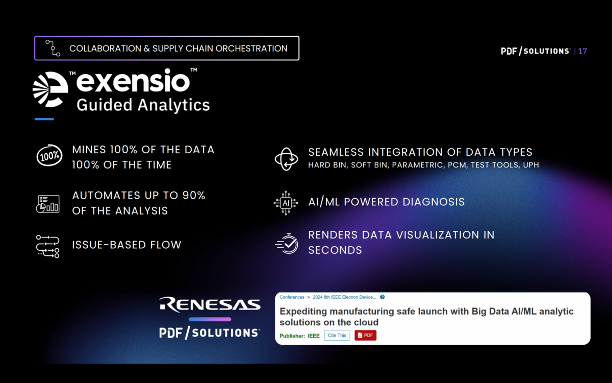
Source: PDF Solutions 2025
Enterprise ModelOps: closing the last mile
At the core is Exensio AI / Studio AI, an enterprise ModelOps layer designed to train, deploy, and manage thousands of models using the massive legacy datasets already resident in Exensio. The focus is on closing the “last mile” between analytics and sustained production deployment.
Roadmap capabilities discussed include reusable analytics workflows, bring-your-own-model support, a secure enterprise model registry, and full traceability between training data, models, and outcomes. This approach addresses long-standing challenges around governance, reproducibility, and operational trust.
Data integration and semantic understanding
A second pillar is breaking down silos between yield, design, and equipment data to accelerate root-cause analysis. Conference discussions highlighted persistent gaps, including limited integration with design-diagnosis ecosystems, incomplete equipment telemetry, and AI tools that force engineers to context-switch.
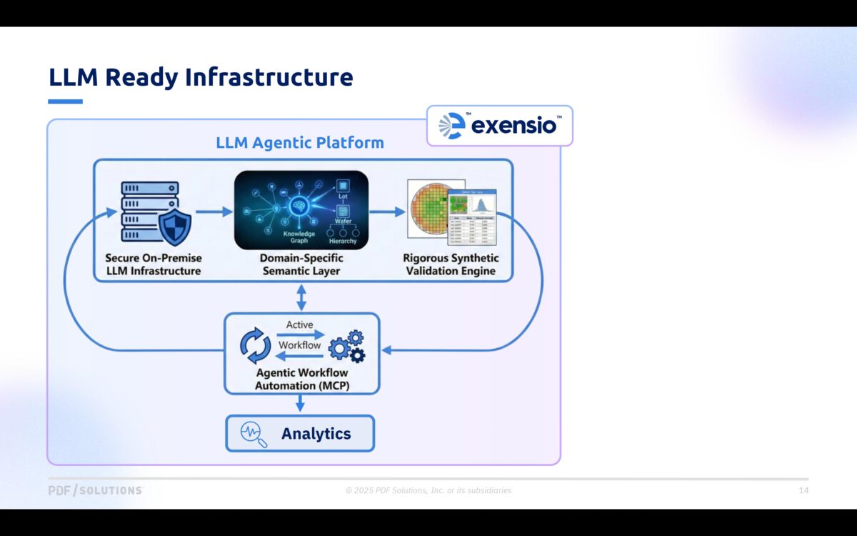
To address this, PDF Solutions is integrating with partners such as Siemens Tessent YieldInsight, combining design-for-test diagnosis data and layout context with Exensio’s manufacturing and test datasets. On top of this, the company is building a semiconductor semantic knowledge graph layer spanning lots, wafers, dies, packages, test structures, and yield metrics.
This pragmatic, evolving semantic layer allows analytics and language models to interpret data in context, selectively incorporating design information where it materially improves diagnosis and decision-making.
Agentic LLM infrastructure with governance by design
The third pillar is an LLM-driven, agentic workflow platform designed for secure, high-stakes environments. PDF Solutions is implementing on-premise and air-gapped LLM infrastructure so sensitive IP and yield data remain behind the customer’s firewall.
Built on the Model Context Protocol, Exensio is evolving into an engineer-directed agentic system, assisting with multi-step workflows, from ingesting raw logs to generating diagnostics and guiding engineers toward likely root causes. A synthetic validation engine stress-tests these workflows before production deployment.

Customer value in practice
A customer deep dive illustrated how this PDF Solutions’ strategy translates into value during yield ramp and failure analysis. In modern GPUs and complex SoCs, scan testing generates rich defect information, but scan diagnosis, layout review, and volume data analysis have traditionally lived in fragmented tools.
By integrating Siemens Tessent Diagnosis and YieldInsight directly into Exensio MA, PDF Solutions provides a single environment for analytics, visualization, machine learning, and layout-aware investigation.
From New Product Introduction (NPI) to High Volume Manufacturing (HVM)
This unified platform turns what was historically an NPI-focused, expert-driven flow into an HVM-ready capability that scales across products, sites, and teams. Engineers gain faster access to diagnosis results and layout context, increasing the likelihood of pinpointing failure locations and shortening the path to corrective action.
Because it is built on Exensio’s scalable data and AI infrastructure, the solution can be deployed across on-premise and cloud environments and extended with agentic capabilities as customers mature. This enables applications such as automated triage, pattern-based excursion detection, and conversational copilots to be grounded in governed data.
Summary
Across John Kibarian’s industry framing, the company’s platform roadmap, and the Siemens use-case deep dive, a consistent theme emerged. The next era of semiconductor manufacturing will be won by companies that treat data, AI, and collaboration as a unified operating system, not a collection of disconnected tools.
PDF Solutions’ mission is to provide a backbone that is semantic, agentic, and secure. With this, customers can turn the growing avalanche of manufacturing and design data into smarter, faster, and more collaborative decisions at scale.
The content of the 2025 PDF Solutions Users Conference can be found here:
https://www.pdf.com/company/pdf-solutions-users-conference/
In January, look out for a post featuring excerpts from a PDF Solutions Conference dinner chat between John Kibarian, CEO of PDF Solutions, and Tom Caufield, Executive Chairman of GlobalFoundries.
Also Read:
PDF Solutions Charts a Course for the Future at Its User Conference and Analyst Day
PDF Solutions Calls for a Revolution in Semiconductor Collaboration at SEMICON West
PDF Solutions Adds Security and Scalability to Manufacturing and Test
Share this post via:


Comments
There are no comments yet.
You must register or log in to view/post comments.