
Overview
Sarcina Technology is a U.S.-based semiconductor packaging specialist offering integrated post‑silicon services from package design through test hardware and production. The company helps semiconductor firms outsource advanced packaging and test solutions for high‑pin‑count, high-performance chip systems.
History & Foundation
Founded in October 2011 in Palo Alto, California, Sarcina was established to centralize complex packaging services under one roof. Its founder and CEO, Dr. Larry Zu—an industry veteran with experience at Bell Labs, DEC, Intel, and TSMC—has led the company’s expansion from traditional package design into full test and production services over more than a decade
Core Offerings & Technology
-
Wafer‑In Product‑Out (WIPO) Services – End-to-end advanced package design, signal/power integrity simulation, final test hardware, wafer sort, and device qualification.
-
High‑Density Package Solutions – Expertise in packaging ASICs with high pin counts and high data-rate interfaces tailored for high-performance computing and AI chip applications
-
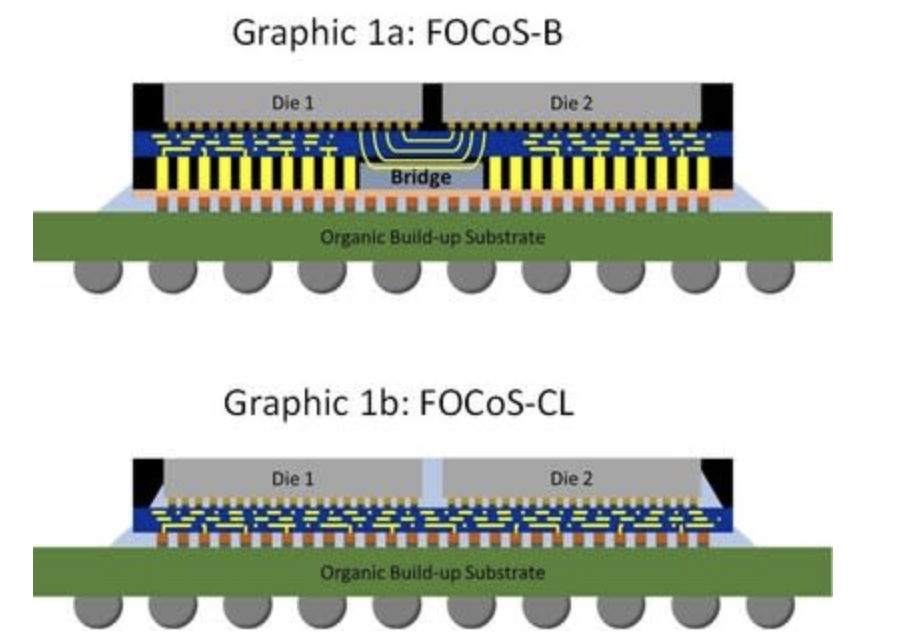
AI Packaging Platform – Uses FOCoS-CL (Fan-Out Chip-on-Substrate, Chip-Last) assembly with UCIe-A interposer technology to support chiplet-based AI designs, enabling up to 64-bit per module at 32 GT/s and integration of LPDDR5X/6 or HBM3E memory
-
Co-Packaged Optics (CPO) Design – Integrated photonic and electronic package solutions that directly combine ASICs and silicon photonic ICs in a single module, improving latency, bandwidth, power and alignment precision for data center connectivity applications
-
Cryogenic Packaging Solutions – Designs capable of operating reliably at extreme low temperatures (e.g., 77 K) for quantum computing memory applications, in collaboration with partners like SureCore
Markets & Applications
Sarcina’s services are tailored to:
-
Generative AI, data center compute, and edge accelerator chip makers needing advanced packaging with high memory integration.
-
High-speed networking and server systems transitioning to co-packaged optics.
-
Emerging quantum computing firms and memory developers requiring cryogenic-capable packaging solutions.
Competitive Strengths
-
Turn‑key approach – Integrated solutions covering packaging, wafer sort, test‑program hardware and qualification.
-
High first‑tape‑out success – Reliable designs with minimal iterations, enabled by deep integrity simulation and layout expertise
-
Cross-disciplinary innovation – Combines electrical, optical, thermal, and mechanical design disciplines to deliver high-performance systems-level packages.
-
Chiplet‑ready packaging – Supports modular, scalable die-to-die interconnection architectures using UCIe-A and package interposers for flexible memory and compute integration.
Leadership
-
Dr. Larry Zu (Founder & CEO) — A seasoned semiconductor engineer with a Ph.D. in Electrical & Computer Engineering, known for leading packaging designs at Bell Labs, Intel, DEC, and TSMC, and credited with nearly 1,000 successful package tape‑outs in his career
Vision & Mission
Sarcina Technology aims to be the premier global provider of advanced, customizable semiconductor packaging and post-silicon services for emerging chip architectures. Its mission is to accelerate customer design cycles and enable scalable high-performance systems by integrating package engineering, chiplet connectivity, memory integration, and testing under one expert roof.
Sarcina Technology on SemiWiki
Share this post via:


Comments
There are no comments yet.
You must register or log in to view/post comments.