

GlobalFoundries Inc. (GF) is a leading pure-play semiconductor foundry that manufactures feature-rich, mature, and specialty process nodes rather than pursuing cutting-edge logic like 3nm or 2nm. GF focuses on automotive, IoT, wireless, defense, aerospace, and RF communications, positioning itself as a critical global supplier in the diversified semiconductor value chain.
Headquartered in the United States and with multiple fabs worldwide, GF is known for its reliable long-life process nodes, commitment to U.S. and European sovereignty, and strategic importance to secure semiconductor supply chains.
Fast Facts
| Item | Details |
|---|---|
| Name | GlobalFoundries Inc. (GF) |
| Founded | March 2009 |
| Headquarters | Malta, New York, USA |
| CEO | Tim Breen (since April 2025) |
| Stock | NASDAQ: GFS (IPO in October 2021) |
| Employees | ~13,000 (as of 2025) |
| 2024 Revenue | $6.75 billion |
| Ownership | Majority-owned by Mubadala Investment Company (UAE sovereign wealth fund) |
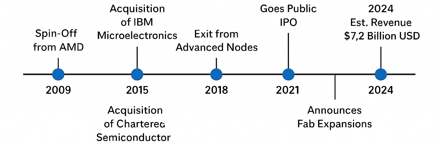
History
| Year | Event |
|---|---|
| 2009 | Founded via spin-off from AMD’s manufacturing arm |
| 2010 | Acquired Chartered Semiconductor (Singapore) |
| 2015 | Acquired IBM Microelectronics (including East Fishkill fab and SOI technologies) |
| 2018 | Exited advanced node race (7nm and below); focused on feature-rich platforms |
| 2021 | Went public on the NASDAQ (Ticker: GFS) |
| 2023–25 | Announced capacity expansions in U.S., Singapore, and Germany |
Foundry Strategy
GlobalFoundries operates a “More-than-Moore” strategy focused on application-optimized technologies rather than chasing raw transistor scaling. It emphasizes:
-
Mature nodes: 180nm, 130nm, 90nm, 55nm, 40nm
-
RF SOI & Silicon Photonics
-
FD-SOI (22FDX / 12FDX)
-
Embedded Non-Volatile Memory (eNVM)
-
Power Management (BCD, GaN)
-
Automotive-grade semiconductors
-
Secure and defense-grade semiconductors
Global Fab Footprint
🇺🇸 United States
-
Fab 8 – Malta, New York (300mm, 14/12nm FinFET, 22FDX)
-
Fab 9 – Essex Junction, Vermont (200mm, acquired from IBM)
-
Fab 10 – East Fishkill, New York (now sold to onsemi, but GF retains IP and technology rights)
🇸🇬 Singapore
-
Multiple 200mm and 300mm fabs focused on mixed-signal, RF, power, and NVM processes.
🇩🇪 Germany
-
Fab 1 – Dresden, 300mm site producing 22FDX and 40/28nm processes.
Future Expansion
-
Dresden MegaFab expansion (with EU funding)
-
Malta Fab 8.2 expansion (CHIPS Act-funded)
-
Continued investment in Singapore new 300mm fab module
Key Technologies
| Platform | Description |
|---|---|
| 22FDX/12FDX | Fully Depleted SOI – low power, low leakage for IoT and wireless |
| FinFET | 14nm/12nm node for performance-sensitive products |
| RF SOI | Industry leader in RF switch and front-end module manufacturing |
| Auto & Power | Automotive-grade process reliability; BCD for power ICs |
| eNVM | Embedded flash and MRAM options for industrial and automotive |
| Secure Foundry | Trusted foundry certifications for U.S. DoD contracts |
Business Focus
GlobalFoundries serves more than 200 customers, including:
-
Qualcomm (RF)
-
NXP (automotive & industrial)
-
Broadcom
-
General Motors
-
Lockheed Martin
-
Bosch
-
STMicroelectronics (for FD-SOI collaboration)
Applications include:
-
5G RF front ends
-
AIoT edge computing
-
Electric vehicle (EV) components
-
Secure aerospace & defense electronics
-
Industrial automation and robotics
Financial & Strategic Outlook
-
IPO (2021) raised $2.6B, giving GF a market cap of ~$30–40B as of 2025.
-
Received U.S. CHIPS Act incentives for Fab 8 expansion.
-
Key partner in U.S. and EU semiconductor sovereignty efforts.
-
Pledged carbon neutrality by 2050.
Leadership
Executive team
-
Tim Breen — Chief Executive Officer
-
Niels Anderskouv — President & Chief Operating Officer
-
John Hollister — Chief Financial Officer
-
Gregg Bartlett — Chief Technology Officer
-
Mike Hogan — Chief Business Officer
-
Saam Azar — Chief Legal Officer
-
Pradip Singh — Chief Manufacturing Officer
-
Samuel Vicari — Chief Customer Officer
-
Pradheepa Raman — Chief People Officer
-
Brad Clay — Chief Information Officer
Board leadership
-
Dr. Thomas Caulfield — Executive Chairman
-
David Kerko — Lead Independent Director
-
Directors: Tim Breen, Marc Antaki, Glenda Dorchak, Martin L. Edelman, Camilla Languille, Jack Lazar, Elissa Murphy, Carlos Obeid, Dr. Bobby Yerramilli-Rao
Challenges
| Challenge | Details |
|---|---|
| Advanced Node Gap | No 7nm, 5nm, or 3nm offerings—less competitive in mobile & HPC |
| Customer Dependency | Relies heavily on automotive and RF verticals |
| Geopolitical Complexity | Navigates U.S., EU, and UAE interests in parallel |
| Talent Competition | Struggles to recruit leading-edge engineers from TSMC/Intel/Samsung |
Summary
GlobalFoundries plays a unique and essential role in the semiconductor ecosystem by focusing on feature-rich, mature, and reliable process technologies. As governments diversify supply chains and prioritize semiconductor security, GF has become a strategic pillar in U.S. and European industrial policy—even without cutting-edge nodes.
Also Read:
Share this post via:


The Packaging PDK Is the Missing Layer for Co-Packaged Optics