You are currently viewing SemiWiki as a guest which gives you limited access to the site. To view blog comments and experience other SemiWiki features you must be a registered member. Registration is fast, simple, and absolutely free so please, join our community today!
Randy Caplan is co-founder and EVP of Silicon Creations. For over 18 years, Randy has helped to grow Silicon Creations into a leading semiconductor IP company with more than 500 customers in over 20 countries, and nearly 100% employee retention. Silicon Creations’ designs have been included in over 1500 mass-produced chips from 3nm to 350nm, from which more than ten million wafers were shipped. Randy’s earlier career includes developing high-speed data transceivers at Agilent Technologies and as a Senior Design Engineer at MOSAID, where he contributed to high-performance silicon IP clocking and interface products.
Tell us a little bit about yourself and your company.
Silicon Creations is a mixed-signal IP provider, specializing in low-risk, high performance clocking solutions (PLLs) and high speed data interfaces (SerDes). We offer designs in every foundry (TSMC, Samsung, GF, Intel, Rapidus, UMC, SMIC, and more…), and every process node (2nm up to 180nm, all inclusive). We were founded in 2006, are ISO9001 certified, and after 18 years, still have close to 100% employee retention.
What was the most exciting high point of 2024 for your company?
Passing ten million (TSMC) wafers shipped using our IP. Also, we passed our 1000th production license of our Fractional SoC PLL IP.
We developed and taped out a portfolio of advanced-node TSMC IP including multiple PLLs, free-running oscillators, low-noise IOs, and temperature sensor IP. We also developed select 2nm PLLs with multiple other foundries including Samsung, Intel, and Rapidus.
What was the biggest challenge your company faced in 2024?
Simultaneously developing IP in all the leading process nodes (TSMC, Samsung, Intel, Rapidus). This required new design techniques to support core-device-only requirements in GAA (gate-all-around) nano-sheet / nano-wire processes.
How is your company’s work addressing this biggest challenge?
Chip development costs in advanced nodes have gone up exponentially. We provide a substantial portfolio of low-risk, proven, foundational IP which helps enable our customers to get their designs right the first time. Our advanced design and verification flow enables fast iteration and re-verification in processes where PDKs are frequently changing. This ensures we’re not the bottleneck in our customers’ development schedule.
What do you think the biggest growth area for 2025 will be, and why?
We’re seeing growth in many parallel market segments including AI accelerator chips, crypto mining, and automotive. Customer tapeouts in advanced nodes (5nm and below) are picking up. We’re even seeing early interest in sub-2nm nodes. Due to long chip development schedules and fab times in advanced nodes, our IP sales tend to be a strong leading indicator of chip sales one to two years in the future. We don’t have first-hand knowledge of the end market forces, but we can infer from our IP sales which semiconductor market segments are seeing increased investment now.
How is your company’s work addressing this growth?
We use an advanced IP design flow, leveraging the latest EDA flows from Siemens, Synopsys, Cadence, Silvaco, and others. This helps to reduce IP development time, improve simulation-to-silicon correlation, and ensure our customers have the foundational blocks they need to build their high-performance chips.
What conferences did you attend in 2024 and how was the traffic?
All TSMC shows, ICCAD (China), DAC and many other foundry and EDA events (Samsung, GF, Intel, Siemens U2U, CadenceLive). Traffic was especially strong at TSMC and ICCAD, but we also had a good turn-out at our booth for the other events as well.
Will you attend conferences in 2025? Same or more?
Silicon Creations attended over 30 trade shows / conferences in 2024, and expects to attend a similar number in 2025…
How do customers engage with your company?
We already work with 16 of the top 20 TSMC customers, and over 500 companies overall. For new inquiries, please send an email to sales@siliconcr.com, or come to our booth at any trade show.
Silicon Creations is a self-funded, leading silicon IP provider with offices in the US and Poland, and sales representation worldwide. The company provides world-class silicon intellectual property (IP) for precision and general-purpose timing (PLLs), oscillators, low-power, high-performance multi-protocol and targeted SerDes and high-speed differential I/Os for diverse applications including smart phones, wearables, consumer devices, processors, network devices, automotive, IoT, and medical devices. Silicon Creations’ IP is proven and/or in high-volume mass production in process technologies up to the most advanced available in the industry.
Part 2 of 2 – Performance Validation Across Hardware Blocks and Firmware in SoC Designs
Part 2 explores the performance validation process across hardware blocks and firmware in System-on-Chip (SoC) designs, emphasizing the critical role of Hardware-Assisted Verification (HAV) platforms. It outlines the validation workflow driven by real-world applications, and best practices for leveraging HAV platforms to ensure comprehensive performance validation and meet evolving design demands. Part 1 is found here
Performance Validation Models in the SoC Verification Flow
It is crucial to distinguish between performance validation and architectural exploration, as these processes serve different purposes in the design and development cycle. Architectural exploration focuses on selecting the optimal SoC architecture to achieve specific design goals, such as maximizing performance or minimizing silicon area. In contrast, performance validation evaluates the actual performance of an architectural implementation to ensure it meets the intended specifications and operational requirements.
Performance validation is a comprehensive, multi-phase process that begins at the architectural level and progressively refines through the abstraction hierarchy, culminating in post-silicon validation. Each stage ensures the design remains aligned with performance expectations, mitigating risks before final production.
In the pre-silicon phase, performance validation relies on two distinct abstraction models, in contrast to software validation, which can utilize hybrid modeling techniques:
Approximately Timed (AT) Models: These models are used for early performance estimations, emphasizing functional correctness and coarse-grained timing analysis. Typically written in SystemC, AT models help identify potential bottlenecks and provide an initial understanding of the system’s behavior.
Cycle-Accurate (CA) Models: Offering detailed, clock-level timing accuracy, CA models are essential for evaluating critical performance metrics such as cycles per second, frames per second, or packets per second. These metrics are key to assessing system efficiency and ensuring the design meets specified requirements. CA models are also implemented in SystemC. When CA models are unavailable, performance validation must be conducted using cycle-accurate RTL simulations.
As the design progresses from abstraction to physical implementation, the final phase of performance validation occurs during silicon engineering sample (ES) testing after the pre-silicon stage. This stage ensures that the actual silicon meets performance expectations under real-world operational conditions. It serves as the ultimate verification step to confirm that the device functions as intended and satisfies all specified requirements before mass production.
By differentiating these processes and employing appropriate tools at each stage, developers can optimize both the architecture and performance of their designs, reducing time-to-market and improving reliability.
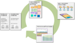
As the following figure shows, that analysis first happens at the architectural level (AT modeling) where it is explored if a particular architecture can support a certain workload performance using models of workload and architecture, given the constraints that a multi-die implementation will pose. Later at the CA level the exact performance is measured using the actual software workload on the detailed target architecture.
Fig 1. Analyzing Performance KPIs for complex, multi-die designs at the architecture level.
Performance Validation Methods
Performance validation can be performed at two key points: at the I/O design boundary or within the design itself.
Performance Analysis at the DUT I/O Boundary
This method measures performance externally, using the Design Under Test (DUT) interface. It often involves PCI Monitors: to assess DUT performance at the pin level, enabling precise, cycle-accurate testing. Real applications, such as I/O meter tools are executed in virtual environments to simulate traffic. Cycle-Accurate Data Capture: Monitors at the RTL pin level collect detailed performance metrics, providing insights into the DUT’s behavior under test conditions.
Performance Analysis Inside the DUT
Internal analysis is employed to diagnose issues. This approach involves DPI calls and internal monitors: These tools, combined with post-simulation scripts, help pinpoint performance bottlenecks within the system. Performance tracking: data is typically logged and managed in spreadsheets, with a framework of test cases designed to evaluate specific performance metrics.
Role of Monitors
Monitors play different roles, with some designed for transaction-level debugging and others focused solely on performance validation. The distinction is crucial.
In performance validation, the design clocks must remain running without interruption. Parameters analyzed are typically minimal and focused on transaction counts, such as read latency, the gap between two reads, read-after-write timing, and other performance indicators. Monitors check these metrics on the bus to assess performance.
In contrast, transaction-level debugging involves snooping the entire bus and tracking each transaction, often causing delays. For performance validation, the analysis is more streamlined, focusing on gaps between transactions, response latency, bandwidth usage, throttling, and backpressure management.
Performance Validation: The Role of HAV
Meeting verification requirements under realistic stress conditions necessitates the use of HAV platforms instead of traditional RTL simulation. Unlike RTL simulations, which are slow and impractical for running actual performance traffic, HAV platforms offer an efficient solution for thorough stress testing and performance measurement. HAV makes it possible to measure performance under real-world software and workload conditions.
In addition to supporting software bring-up and system validation, HAV platforms are increasingly driven by the need for precise power and performance analysis. HAV excels in measuring critical metrics like throughput and latency by counting clock cycles with exact precision. Testing these metrics requires real-world application payloads, as simple directed test cases are insufficient. A high-speed system is essential to execute complex application workloads effectively, ensuring meaningful and reliable performance evaluations.
To meet these demands, up to one-third of HAV resources are often dedicated solely to performance measurement. This allocation highlights the pivotal role HAV platforms play in modern performance validation, enabling engineers to address the complexities of today’s high-performance systems.
Performance Validation at the Firmware Layer
HAV plays a crucial role in performance tuning at the firmware level, an area gaining significant attention. For example, SSD providers1 frequently release updated firmware specifically designed to enhance performance, leveraging HAV to ensure these improvements are both measurable and reliable.
Firmware testing on actual silicon has become a vital part of performance validation frameworks. A main reason for adopting HAV is to enable the execution of firmware, which is not feasible in traditional simulation environments. The faster the validation platform, the better the ability to run real firmware effectively.
Running real firmware requires a PHY (physical layer). While PHY models do not include the full physical/analog properties, they facilitate the optimization of register access and other firmware interactions that impact performance. This early tuning can have a significant effect on overall system performance and efficiency.
The primary purpose of using a PHY model is to optimize firmware performance in conjunction with pre-silicon RTL, not to modify the RTL itself. This approach shifts the focus from measuring and validating the design’s performance to evaluating and enhancing system performance, including firmware, before chip release. This shift-left strategy allows teams to begin performance optimization much earlier in the development cycle.
Getting to the best performance
As outlined above, achieving optimal performance involves two key steps.
First, defining the optimal architecture to meet performance goals. This requires approximately timed models and a simulation and analysis framework that supports modeling and rapid simulation of various architectures and scenarios. Synopsys Platform Architect has become the industry-standard tool for this task, offering robust capabilities for exploring and optimizing system-level architectures.
Second, performance validation through emulation. The Synopsys ZeBu product family is critical for this stage, providing the fastest emulation performance available. Additionally, its extensive support for performance validation solutions enables both internal and external measurements while ensuring the ability to run accurate models of Synopsys PHY IPs. These capabilities are instrumental in delivering high-confidence validation results.
The question isn’t whether design teams should use these advanced tools, it’s how much time and resources they should invest in them. Greater investment in pre-silicon performance analysis and validation significantly increases the likelihood of delivering silicon with highly differentiated capabilities.
Read Part 1 of this series – Essential Performance Metrics to Validate SoC Performance Analysis
Tell us a little bit about yourself and your company.
The PQShield team helped define the new PQC (post-quantum cryptography) standards that will be used to replace current encryption that is vulnerable to attack by quantum computers. Now, we work with international blue-chip organizations, disruptive scale-ups, and national bodies throughout the technology supply chain to deliver the secure transition to quantum safety.
I have worked in hardware security for the past 20 years across Asia, Europe, the US and Middle East in industry and academia. In a time when quantum computers will soon be able to break current cryptography methods, I am focused on empowering organizations, industries and nations with the quantum-resistant cryptography solutions they need to protect themselves.
What was the most exciting high point of 2024 for your company?
This year was a momentous one in the history of post-quantum cryptography with the publication of the NIST PQC standards FIPS 203, FIPS 204, and FIPS 205. This marked the culmination of eight years of hard work from the global cryptographic community and was also a high point for the PQShield team, who contributed to all three of the final standards.
But more exciting is what comes next. The NIST standards have fired the starting gun for the PQC transition, as businesses armed with these standards now have the tools to implement their PQC transition roadmaps. After years of discussions around crypto discovery, we can finally focus on the secure implementation of PQC, an area particularly close to my heart – particularly looking at hardware implementations and resistance to side-channel and fault injection attacks (SCA and FI).
What was the biggest challenge your company faced in 2024?
The challenge we face is that we are replacing RSA, ECDSA and similar encryption – well understood and thoroughly tested over many years – with PQC, which is fundamentally new, based on different mathematics, and not a like-for-like replacement. There will be hurdles to cross as we work to deliver the most fundamental upgrade to our cybersecurity infrastructure in a generation.
As anyone in cybersecurity knows, attackers are always working to find new vulnerabilities and methods to crack encryption. As we roll out PQC across our digital infrastructure, our work is focused on ensuring that every line of code we write, every mathematical problem we solve, and every interaction we make is focused on one specific goal: keeping us all one step ahead of the attackers.
How is your company’s work addressing this biggest challenge?
A significant milestone for us was the certification of our PQCryptoLib, PQShield’s hybrid cryptographic library, which has achieved FIPS-140-3 certification under the NIST CMVP process.
This represents a huge three-year team effort. PQCryptoLib is the library that underpins many of PQShield’s products – including the PQPlatform hardware IP family. While there will be many iterations of our products put forward for certification, this achievement represents a quality threshold that can now be attained by PQC.
Off the back of this effort, towards the summer of 2024 we introduced our first fully functional PQC silicon test chip. By building our own ASIC, we can now demonstrate and test our IP in the way that a customer will use it. We’re able to evaluate its operation in real detail, looking at how to be compliant against the NIST standards and perform security testing in a way that would be practically difficult on a customer product deployed in the field.
As we look forward to next year, we will start to see hardware manufacturers bringing new PQC products to market and we are primed as key partners to help them on that journey.
What do you think the biggest growth area for 2025 will be, and why?
For the vast majority of organizations, their ability to transition to PQC will be dependent on their supply chain’s ability to deliver PQC secure products. Therefore, businesses that sit at the foundation of the supply chain – particularly semiconductor manufacturers – are primed for growth and disruption.
As our lives are increasingly digitized through the cloud, businesses operate more advanced industrial IoT, and AI continues to drive demand for high throughput semiconductors, the introduction of PQC enabled hardware is only going to increase demand in this highly competitive sector.
Following the announcement of NIST standards, I expect we will be ending 2025 with quantum security firmly on the agenda of every boardroom in the global technology supply chain.
How is your company’s work addressing this growth?
PQShield is already well placed to help the semiconductor and hardware industries meet this demand. We now have long standing collaborations with Microchip Technologies, AMD and Lattice Semiconductors among others to help develop PQC solutions. Our extensive product suite is helping customers to implement PQC into their design pipelines to ensure quantum secure products reach the market in the new year.
To help us meet this growing demand, we have significantly expanded our corporate function to support global expansion across Europe, the US and Asia. This includes additions to our executive and strategic advisory board, with Antonio J. Viana (BrainChip, Arteris, Parsley, former Arm executive) joining as Non-Executive Director alongside three new additions to our strategic advisory board to accelerate growth into 2025: Mike Muller (co-founder and former CTO, Arm), Rose Schooler (former CVP, Intel, and current Arm board member), and Ian Drew (former chairman at Foundries.io, and CMO at Arm).
Knowing we’re on the precipice of the biggest technological transition in a generation, we’re confident that we have the team and the products to help the market grow in 2025.
What conferences did you attend in 2024 and how was the traffic?
Events are a key opportunity for us to meet our customers and help them to address their questions and concerns around PQC. Two big tentpole events for us last year were Mobile World Congress (MWC) in Barcelona and RSA in San Francisco. At both, we were able to showcase our collaboration with AMD and demonstrate how PQShield’s PQPerform PQC hardware accelerator was installed on the programmable logic of the AMD Versal Adaptive SoC.
Will you attend conferences in 2025? Same or more?
We will be back at MWC and RSA again next year and will be showing how our products have progressed following the publication of NIST’s standards.
Our team loves to get out and about and we have over 20 conferences we plan to attend just in the first half of 2025 alone! To name a few we have CES, Embedded World, CyberUK, DAC, DSEI 2025 and many others.
How do customers engage with your company?
You can connect with us on LinkedIn where we regularly highlight the events we’re attending as well as our latest research. We also have a monthly newsletter that shares the latest developments in PQC and at PQShield.
Get in touch if you have any concerns about planning your own PQC transition as the industry enters the execution phase. Our team has experience across the full spectrum of industry sectors and potential use cases, and is already advising both governments and global enterprises on this transition.
Additional questions or final comments?
Quantum-safe secure boot and PQ/T hybrid requirements are the main challenges moving forward.
The foundation of modern cybersecurity lies in the secure boot process, ensuring only trusted and authenticated software runs on a device. By validating code integrity through cryptographic signatures, secure boot upholds the Confidentiality, Integrity, and Availability triad, acting as the first line of defense against tampering, malware, and unauthorized changes.
The European Union and relevant agencies, such as ANSSI and BSI, advocate for a Post-Quantum/Traditional (PQ/T) hybrid cryptographic model, combining quantum-resistant algorithms with traditional cryptography for added resilience. Implementing quantum-safe secure boot remains challenging due to the performance, scalability, and compliance trade-offs of PQ/T solutions.
I am excited that we are developing a flexible Root of Trust to address this challenge, enabling diverse platforms—embedded systems, edge devices, and Critical National Infrastructure—to transition to quantum-resistant architectures seamlessly.
PQShield comprises a world-class collaboration of post-quantum cryptographers, engineers, and operators. We’ve helped shape all of the first international PQC NIST standards, and we were the first cybersecurity company to develop quantum-safe cryptography on chips, in applications, and in the cloud.
Tell us a little bit about yourself and your company.
Larry Zu
I’m Larry Zu, Founder and CEO of Sarcina Technology. I’ve grown Sarcina from just designing packages for a few small companies to handling the entire post-silicon ecosystem, including package design, assembly, testing, qualification and production services for the top semiconductor companies in the world. I began my career at Bell Labs, before moving to DEC, Intel, and TSMC. Along the way, I acquired deep skills on how to develop successful products including the Alpha, Itanium 2, Pentium 4, and XBOX 360 microprocessors.
Over my career, I have taped out nearly 1,000 packages with a greater than 99% first tape-out success rate. I’ve applied those skills to build Sarcina, a company that works with the world’s top foundries to ensure high quality products. We manage from the simplest to the most complex of packages. Companies forward their wafers from their foundries and Sarcina does the rest. Wafers in, packaged chips out.
What was the most exciting high point of 2024 for your company?
There were many great successes in 2024, so this is a difficult question. If I had to pick one, perhaps I would cite our work on Bump Pitch Transformers (BPT). I know it’s an odd name, but what this work does is reduce the cost and complexity of 2.5D package designs.
Current advanced 2.5D packaging uses a substrate to transpose a chip’s microbump pitch from 40-50 micrometers to the package’s 130 micrometer bump pitch. This is typically done with a silicon TSV (through-silicon via) interposer. These substrates are very expensive, in short supply, and complex to design, resulting in lead-time and cost challenges for many advanced designs.
Our BPT approach uses RDL interconnect or silicon bridge technologies, replacing silicon TSV interposers with more cost-effective re-distribution layers (RDL). This architecture is ideal for homogeneous and heterogeneous chiplet integration, targeting high-performance computing (HPC) devices for AI, data center, microprocessor, and networking applications.
What was the biggest challenge your company faced in 2024?
Our biggest challenge is actually not a technical one. Sarcina’s strength and fundamental differentiation is our ability to complete high-performance engineering projects. Over the past 12 years, Sarcina has taped out more than 100 packages, all first-time successes. We’ve never re-taped out a single package.
The challenge is to get the word out to more companies who can benefit from our capabilities. We can help small to mid-sized ASIC companies and large system houses be more successful.
How is your company’s work addressing this biggest challenge?
I personally do a lot of presentations at many trade shows and industry events to help spread the word about Sarcina’s Application Specific Advanced Package (ASAP) Service. Our work here on SemiWiki is also a key part of that strategy.
What do you think the biggest growth area for 2025 will be, and why?
Advanced packaging is now setting the trend for the next level of innovation. The know-how to integrate multiple devices in an advanced package provides the margin of victory. Sarcina is at the forefront, enabling these trends.
There will be growth in many areas as a result. Some markets we are currently enabling include AI, networking, data center, high-speed comms, and medical.
How is your company’s work addressing this growth?
We continue to build more advanced flows that embody our substantial experience. Our partnerships also help to expand our reach and impact. The work we are doing with Keysight is an example of this. So is the work we are doing with Intel Foundry Services (IFS) Accelerator Design Services Alliance.
What conferences did you attend in 2024 and how was the traffic?
We attended quite a few events in 2024:
Chiplet Summit
OFC (Optical Fiber Communications)
IEEE MTT-S International Microwave Symposium
Silicon Catalyst Spring Portfolio Conference
Design Automation Conference (DAC) (I was a speaker at the Keysight Theater)
All these conferences are packed with people because they address hot topics in high performance computing and communication for AI applications inside a semiconductor ASIC chip. As semiconductor packaging becomes more and more important to build advanced ASIC chips, we observe more traffic to our booth during these conferences.
Will you attend conferences in 2025? Same or more?
We plan to attend similar shows in 2025, with some possible additions. You can visit https://sarcinatech.com/upcoming-events/ to see the latest plans we have for show attendance.
How do customers engage with your company?
You can certainly stop by and visit us at the shows we will attend. You can also reach out to us on our website here: https://sarcinatech.com/contact/. We’ll respond quickly and work with you to define how we can make you more successful.
Additional questions or final comments?
Semiconductor technology is evolving rapidly. Monolithic integration is being replaced by complex multi-chip system in package design. These designs represent substantial challenges with many new effects to be modeled and tamed. Sarcina has the experience, skills and track record to help you overcome these challenges. Give us a call and find your margin of victory.
Chouki Aktouf is Founder & CEO of Defacto Technologies and Co-Founder of Innova Advanced Technologies. Prior to founding Defacto in 2003, Dr. Aktouf was an associate professor of Computer Science at the University of Grenoble – France and leader of a dependability research group. He holds a PhD in Electric Engineering from Grenoble University.
Tell us a little bit about your company.
We provide since more than two decades innovative SoC design solutions for RTL designers and SoC architects. Defacto’s SoC Compiler tool is becoming the “De Facto” software to build large SoCs pre-synthesis by including not only RTL but also IP-XACT and design collaterals such as UPF and SDC. The Physically awareness of the Defacto tool strengthens its market positioning to meet aggressive PPA goals. The company is also known by its high-quality support which is provided to the end-users and also the innovation Defacto brings every year to the market to help building SoCs faster and cheaper.
What was the most exciting high point of 2024 for your company?
The main accomplishment of Defacto was to position as a real leader in the front-end SoC integration, when having RTL but not only. IP-XACT, UPF, and SDC also need to be considered towards better efficiency, and cost.
What was the biggest challenge your company faced in 2024?
In 2024, one of the biggest challenge was to succeed in R&D projects considering AI technologies. In the new Defacto products, we will be announcing AI-based automation to confirm our tool as the De Facto solution for SoC creation pre synthesis and help designers even with less expertise to benefit from the tool.
How is your company’s work addressing this biggest challenge?
We work closely with leading R&D teams in France and in Europe to help solving technical challenges.
What do you think the biggest growth area for 2025 will be?
We believe AI-based EDA will be the main topic for the coming year.
How is your company’s work addressing this growth?
The company has engaged since several years with best Research labs in Europe to work closely on advanced AI-based technologies for EDA.
What conferences did you attend in 2024 and how was the traffic?
The main conference we attended this year was DAC. We feel that DAC is coming back from COVID since the past year and we were pleased to see a good affluence, in particular during the first day. We eager to see 2025!
Will you attend conferences in 2025? Same or more?
In 2025 we plan to attend DATE which will be close to our Headquarters in Grenoble, France. Of course DAC will be the main event and we will be announcing big new capabilities. We also plan to attend ITC since we have a regrowth activity around DFT with many news to highlight.
How do customers engage with your company?
The best is either to drop us an email (info_req@defactotech.com) or contact us on website (https://defactotech.com/contact). We are known in the market as highly reactive, in both technical and business sides. So we encourage to contact us to set up presentations, demos and evaluations.
We also have an upcoming Innova Webinar that you can also attend:
There is a revolution happening that is fueled by innovation in areas such as AI, IoT and autonomous driving. These new systems put incredible stress on next-generation semiconductor technology. Faster processing, higher density and lower latency must all be delivered with reduced power and thermal profiles. One technology has become the centerpiece for much of these advances – memory. And within that discipline the need for dramatically improved embedded non-volatile memory. Synopsys is at the forefront of innovation here. Let’s find out how Synopsys brings embedded memory to the future with its flexible, IP-based compilers.
Embedded NVRAM – The Options
Flash has been the go-to option for embedded non-volatile memory for a long time. But as applications demand much more non-volatile storage and processes shrink below 28nm, flash memory is running out of steam. A new approach is needed to deliver high-speed data collection, transmission, storage, and analysis at scale.
Two emerging technologies are gaining traction – Magneto-Resistive Random Access Memory (MRAM) and Resistive Random Access Memory (RRAM). These embedded memory options deliver the density, capacity, and scalability for next-generation systems. It turns out each is optimized for different applications and use cases. Let’s examine some of the differences.
MRAM: delivers higher reliability and superior power, performance, and area (PPA), even in extreme environments. Initially developed for aerospace applications, it uses an adjustable magnetic layer to maximize storage density. And its exceptional power and performance characteristics are ideal for applications requiring the highest levels of reliability and data integrity.
The technology is useful for vehicles that need over-the-air software updates for example. A consideration for this technology is its sensitivity to strong magnetic fields. This may be mitigated with physical placement constraints or shielding in certain environments, adding complexity for some applications.
RRAM: is still in the early stages of market awareness and adoption. This technology uses a dielectric layer to store data. It isn’t sensitive to magnetic fields like MRAM, but it is less reliable in extreme environments.
Low cost and energy consumption combined with high density and scalability make RRAM a good choice for IoT devices, wearables, in-room sensors, and other applications requiring cost, power, and space efficiency. RRAM is also being used in automotive applications where environmental conditions can be managed.
Each of these technologies has a place, and design teams need comprehensive access to each to find the best answer. This is where Synopsys brings embedded memory to the future with its flexible, IP-based compilers.
The Synopsys Approach
Thanks to its IP-based compiler solutions, Synopsys can streamline MRAM and RRAM integration. Most suppliers offer a limited set of fixed macro options for embedded memory. With its IP-based compiler solutions, Synopsys provides comprehensive and configurable choices, allowing design teams to instantly build a wide range of macros and precisely match memory sizes and aspect ratios with MCU requirements.
For example, the MRAM Compiler is well-suited for newer applications with simplified power supply requirements, built-in self-test (BIST) and repair, and error correction code (ECC). In addition to accelerating system-on-chip (SoC) integration and time-to-market, it addresses the growing demand for reliable, cost-effective, efficient memory in AI-enabled applications.
The figure below illustrates how configurable MRAM IP provides flexibility for multiple word widths, aspect ratios, and floorplan optimizations.
Configurable MRAM IP
Synopsys is actively developing MRAM in the TSMC 22ULL and TSMC 16FFC processes. The company is also developing automotive MRAM and RRAM compilers in the GlobalFoundries 22FDX process, and they have demonstrated successful MRAM silicon on the 22ULL process, enabling SoC designers with low-risk solutions. Data retention, write endurance, and magnetic immunity testing results have met or exceeded design targets.
Leading foundries have announced roadmaps for additional MRAM and RRAM enablement, including FinFET solutions at 6nm and beyond. Synopsys has stated it will continue advancing next-gen memory technologies and help redefine the future of embedded systems.
Dan is joined by Dr. Walden Rhines. Wally is a lot of things, CEO of Cornami, board member, advisor to many and friend to all. Today he is the Executive Sponsor of the SEMI Electronic Design Market Data report.
Dan explores the recently published report with Wally. Overall growth was 8.8%, a strong number but not as large as prior quarters. However, Wally does report that overall EDA revenue has reached a $20B run rate for the first time, a substantial achievement. Wally and Dan explore the details of the report, including the areas of strong growth and the reasons why. There were two regions that exhibited weaker growth as well. Dan explores the reasons for this with Wally. Some interesting insights about overall market dynamics come out of that discussion.
There are many other insightful discussions, including the strong growth in services and what that can mean for the future of the industry. The views, thoughts, and opinions expressed in these podcasts belong solely to the speaker, and not to the speaker’s employer, organization, committee or any other group or individual
John Chang, founder and CEO of JMEMTEK, combines technical expertise and business acumen to lead the company in addressing critical hardware security challenges. With a PhD candidate in Electro Physics at National Yang Ming Chiao Tung University and dual bachelor’s degrees in Electrical Engineering and Banking and Finance from the Queensland University of Technology, John bridges innovation and strategy seamlessly.
Since founding JMEMTEK in 2022, John has secured over $6 million in funding. His decade-long experience in semiconductor innovation and failure analysis, reinforces JMEMTEK’s position as a leader in hardware security and post-quantum cryptography.
With John’s vision, JMEMTEK continues to drive advancements for industries like FinTech, Defense Tech, and AIoT, shaping the future of secure and scalable technologies in the new quantum era.
Can you tell us about Jmem Technology and its core mission?
Jmem Technology Co., Ltd. is a pioneering company specializing in hardware security IP and IC design services. Our primary mission is to address the growing cybersecurity challenges posed by the advent of quantum computing and emerging threats in the digital age. We focus on developing cutting-edge Post-Quantum Cryptography (PQC) solutions and our foremost technologies on Roof of Trust like J-Physical Unclonable Function (JPUF) technology to deliver robust and scalable security for industries such as FinTech, Defense, and AIoT.
Our vision is simple yet bold: to build a secure digital future by safeguarding critical infrastructures with advanced hardware solutions. This vision drives everything we do, from R&D to partnerships with academia and industry leaders.
What sets Jmem Technology apart in the market?
Jmem Tek stands out because of our dual focus on innovation and practicality. For instance, our proprietary PQC security chip, powered by JPUF technology, not only generates and stores cryptographic keys securely but also enables tamper-proof authentication and secure OTA firmware updates.
Our technology is also designed to be highly scalable, making it adaptable to a wide range of applications—from protecting sensitive data in autonomous vehicles to securing critical systems in defense. Unlike software-based security measures, our hardware-based solutions offer unparalleled protection against cloning, reverse engineering, and other sophisticated attacks. With our chip our solutions can outperformed PQC on software up to few-hundreds times.
Additionally, we have cultivated strong collaborations with globally respected research institutions and corporate partners, including Andes Technology, UMC and co-author with HSSC on Side Channel attack topic. These partnerships validate our technological approach and open doors to new markets and opportunities.
How has Silicon Catalyst supported Jmem Technology’s journey?
Becoming a portfolio company of Silicon Catalyst has been transformative for Jmem Tek. The program offers unparalleled access to mentorship, industry connections, and technical resources. This support has accelerated our product development and market expansion, particularly in the U.S. and Europe.
One of the key benefits is the opportunity to engage with Silicon Catalyst’s extensive network of industry veterans, who provide invaluable insights and guidance as we scale. Additionally, being associated with Silicon Catalyst enhances our credibility as an innovative leader in hardware security, helping us forge stronger relationships with investors and partners.
What industries and applications do you see benefiting most from Jmem Technology’s solutions?
The versatility of our solutions allows us to cater to a diverse range of industries. Our PQC and PUF technologies are particularly valuable for:
FinTech: Ensuring secure transactions and safeguarding sensitive financial data.
Defense: Protecting mission-critical systems and communications against cyber threats.
AIoT: Enabling secure device connectivity and data exchange in smart environments.
As quantum computing continues to evolve, the demand for hardware-based security solutions will only grow, especially in sectors where data confidentiality and system integrity are paramount.
What are Jmem Technology’s plans for the future?
Our immediate goal is to expand our reach into new markets, particularly in Europe and North America, while strengthening our foothold in Taiwan’s semiconductor ecosystem. We’re also focused on advancing our research and development to further enhance the performance and versatility of our PQC and JPUF solutions.
Looking ahead, we aim to deepen our collaborations with strategic partners and academic institutions, leveraging their expertise to refine our technology and explore new applications. Ultimately, our mission is to create a world where every digital interaction is secure, no matter how advanced the threats become.
What excites you most about the future of hardware security?
The rapid advancement of quantum computing poses both challenges and opportunities. While it introduces new vulnerabilities, it also pushes us to innovate faster and smarter. We are excited about the role Jmem Tek can play in this transformative period, helping industries adapt and thrive in the face of unprecedented change, not just secure, but also enhancing the efficiency.
By staying ahead of the curve, we’re not just solving today’s problems—we’re building the foundation for a secure and resilient digital future.
FPGA-based prototyping offers advantages such as high-speed operation, real-world environment testing, and parallel execution that cannot be matched by software simulations alone. It enables developers to validate their designs and initiate software development long before the final silicon is ready. At the same time, prototyping is not merely just an FPGA board, and many factors need to be considered when it comes to rapid and effective implementation. Accelerating FPGA prototyping requires a combination of advanced hardware capabilities, improved design methodologies, efficient debugging tools, and reliable software automation. By leveraging these approaches, engineers can significantly reduce prototyping time while maintaining accuracy and performance.
The Challenges of Prototyping for SoC Development
One of the major hurdles in SoC prototyping is ensuring a realistic testing environment that accurately simulates real-world chip behavior. Additionally, challenges such as managing partitioning for large-scale designs and achieving stable communication between high-speed and low-speed devices add to the complexity. Without the right tools and strategies, development teams face significant delays and increased risk during the prototyping phase, which can impact their ability to meet project deadlines and deliver quality products to the market.
Innovative Approaches to Overcoming Prototyping Hurdles
To address these challenges, several innovative approaches have emerged. Flexible interfaces, such as configurable daughter boards, enable rapid connection to external devices and mimic real-world conditions, allowing developers to validate designs in realistic environments. Speed adapter solutions ensure seamless communication between devices operating at different speeds, which is critical for high-speed interfaces like PCIe or advanced memory standards like LPDDR4/5. Co-simulation tools and reference designs streamline the debugging process by facilitating efficient data exchange and providing pre-validated solutions, reducing the need for custom development. Furthermore, optimized design partitioning and FPGA interconnecting topology play a vital role in managing the complexities of large-scale SoC designs, allowing for iterative mapping of components while maximizing system scalability.
S2C’s Prodigy Prototyping Solutions
S2C’s Prodigy Prototyping Solutions address key challenges in FPGA-based SoC prototyping through flexible hardware, reliable software tools, and streamlined processes.
Flexible Daughter Boards for Seamless Integration
S2C’s Prodigy platform features a vast library of daughter boards supporting applications ranging from communications and SoC to storage and multimedia, including various gigabit Ethernet interfaces, QSFP28/QSFPDD, PCIe, USB, LPDDR4/DDR4, QSPI, EMMC, MIPI D-PHY and HDMI. These modular daughter boards, pre-validated to meet industry standards, simplify system setup and reduce development risks.
Speed Adapter and Memory Models to Bridge the Gap
To overcome the limitations of FPGA-based systems in handling high-speed protocols or the latest memory interfaces, S2C offers speed adapter and memory model solutions to support the device under test in the FPGA environment. This is particularly useful in validating PCIe subsystem not running at real-world speed or advanced memory controllers such as DDR5/HBM, where FPGA vendors often lack suitable PHY IPs. S2C’s PCIe speed adapter can act as a gear shift between two different PCIe speeds while memory models allow customers to validate LPDDR5/DDR5/HBM based memory controllers by bridging gaps to FPGA’s DDR4 PHYs, addressing critical bottlenecks.
High Productivity Toolchain to Streamline Large-scale SoC Designs
Software/hardware co-development with ProtoBridge™: ProtoBridge enables high-throughput data exchange between FPGA prototypes and PC hosts at speed up to 4GB/s utilizing PCIe connectivity. With ready-to-use C APIs on host PC and bridging AXI-4 master/slave IPs running in the DUT, large data such as videos, software applications or operating systems can be uploaded with ease. ProtoBridge is also a critical building block for co-simulation and other co-development applications.
Remote Runtime Management with PlayerPro – Runtime (PPro-RT): Prototyping can be remotely managed and download designs over Ethernet/USB by PPro-RT. With hardware self-tests, virtual I/O tools, and design resource access, it simplifies multi-system management, ensuring effective hardware validation and streamlined firmware testing.
Deep trace and multi-FPGA debugging with PlayerPro – DebugTime (PPro-DT): PPro-DT allows users to pre-select the signals to be observed before compilation and define the trigger conditions to start a data capture. During runtime, the selected signals are captured and stored in an external DDR4 memory for analysis.
Multi-FPGA prototyping with Player Pro – Compile Time (PPro-CT): PPro-CT is a timing-driven partitioning software enables one-click flow from RTL to bitstream, simplifying the steps of large design partitioning with features such as system level STA, high-performance TDM assignment and incremental compilation.
The Benefits of S2C’s Solutions
By providing a near-realistic environment for software validation, S2C’s customers reduce the likelihood of costly rework after silicon fabrication, ensuring a smoother transition to final production. Development teams improve efficiency by leveraging pre-validated components and automated tools, which minimize errors and streamline the prototyping process. The tools also save engineering resources, allowing developers to focus on innovation rather than labor-intensive setup and troubleshooting tasks. Faster time-to-market is achieved as these solutions significantly reduce the time required for debugging and verification, enabling teams to meet tight deadlines.
Summary
The success of FPGA-based prototyping hinges on overcoming several key challenges. By integrating flexible interfaces, speed adapter solutions, advanced co-simulation tools, and high productivity toolchain, S2C’s Prodigy Prototyping Solutions address these challenges head-on. The S2C Prodigy platform empowers development teams to reduce risk, validate designs more efficiently, and deliver products to market faster, making it an invaluable tool in the fast-paced world of chip design.
The moral of today’s story is that to succeed in a late-adopter market, sometimes you just have to wait for the market to catch up (assuming you have a strong early adopter market to buy your product today). I have been working with Arteris for 6+ years now promoting their NoC technology, and there was never any question that they offer significant value for design teams building big, complex systems-on-chip connecting multiple IPs through extensive networks. Such systems include application processors and, more recently, AI systems for automotive applications. Lower-end designs, commonly MCUs, had been more resistant to the benefits of Arteris technology. But as AI, safety, and security are becoming just as important in MCUs as elsewhere, even MCU design teams are rethinking their earlier strategies.
Evolving MCU demands
Historically, MCUs have served relatively bounded objectives like control units in car engines and home appliances. The architecture was comparably simple: an 8-bit processor, memory, peripherals, timers, counters. One initiator, a few targets, easily satisfied by crossbar switch interconnect. Design support teams often built their own generators for this kind of interconnect. A small number even built their own NoC generators to handle more complex system interconnects.
Now even legacy in-house generators are coming under pressure, in part through competitive and regulatory requirements and in part to meet scalability expectations. AI is everywhere, as much in MCUs as anywhere else to support intelligent sensing. Automation demands for smart homes, cars, cities, factories, all require smart MCUs with communication support. Many must also prioritize safety and security, all at very constrained cost and power demand per unit. Cities and factories planning to deploy thousands of devices want unit prices around a few dollars at most and even lower maintenance costs.
MCUs are growing up to meet these needs; now it’s not always easy to tell where MCUs end and SoCs begin. According to Andy Nightingale (VP Product Management and Marketing, Arteris), MCUs span a long tail beyond SoCs, from complex all the way down to simple devices. Simple MCUs still have their uses where cost is more important than adding features (simple toys or basic home thermostats, for example), but above wherever that breakpoint might be, more functions must be supported on-chip and that invariably requires NoC connectivity.
The drivers to mainstream NoCs
What is motivating change at the simpler end of this MCU range? In part, power reduction. Networks burn power even when there’s no traffic, a fact easy to overlook when concentrating on minimizing power in endpoint IPs. This power component alone can be an important overhead, unless you are using a network like Arteris FlexNoC which supports power domain switching and DVFS within the network.
Safety standards have become another driver. If the MCU is going into any safety-critical application (car, aircraft, industrial robotics, …) you must demonstrate compliance to applicable standards, again as much for the network as for the endpoint IP. Arteris has already done the groundwork against both ASIL B and ASIL D for automotive applications.
At higher complexities, many requirements making NoCs essential in SoC design have become just as relevant in MCU design. Support for multiple protocols (AXI, ACE-lite, ACE, CHI, APB, etc.) is unavoidable in designs using both legacy and 3rd party IP, and acceptable performance for systems with multiple initiators and targets is only possible through the packetization offered by NoCs.
AI accelerators, multicore processors, and again performance are pushing new network topologies: mesh, tree, Clos, even crossbars in some cases, demanding NoC generators with track records to provide support across this range. Meanwhile, network standards continue to evolve. In debug and parametric modeling, support for ATB 128-bit trace and now DVM 8.1 have become essential. AMBA 5 now supports “stashing” to improve memory utilization, latencies, and bandwidths, here also requiring support from the NoC generator. High-end goals can only be guaranteed with networks that constantly track these new demands.
For implementation, it is now clear that complex NoC design must be physically as well as architecturally aware right from the outset. Bus widths and serialization options can be optimized early on against rough floorplan concepts and later fine-tuned against realistic floorplans to best optimize area/performance tradeoffs. Just as logical/physical co-design appeared years ago in physical synthesis for block design, now the same need has become unavoidable in full system design.
Strategic planning for scalability
No design is an island, as some reuse expert might have said. What we build today must also factor into tomorrow’s plan for larger or repurposed designs. Or reuse may go in the opposite direction. Auto OEMs may first design a system for the high end of a car range, with intent to deploy the same system or a derated version in lower-end models in the future. In support of these goals, it is necessary to plan for a design infrastructure that can span seamlessly from low-end MCUs to high-end MCUs to SoCs, without need for fundamental network redesign.
Between the intrinsic flexibility of NoC-based networks and physically aware design, Arteris networks can easily span this range (since they are already widely deployed in high-end SoC design flows). Hierarchical NoCs are already as commonplace as hierarchical crossbar switches, so reuse methods are also well-proven. It seems pretty clear that NoC architectures are the way to go for scalability.
You can learn more about this topic HERE, the Arteris non-coherent FlexNoC architecture HERE, and their coherent Ncore architecture HERE.